
The Workhorse Alloy of Low-Temperature Ribbon: Sn32Pb42Bi26 in PV Ribbon Today and Tomorrow
Key points (short version)
- Low melting point: Sn32Pb42Bi26 melts at about 136–143 °C, roughly 40 °C below conventional Sn63Pb37, and is one of today's main production alloys for low-temperature ribbon.
- The value is in the process: its core value is not being "cheaper" but lowering the soldering temperature and reducing thermo-mechanical stress, which makes it a natural fit for HJT and 0BB lamination-soldering processes.
- The weak spot is lead: it contains 42 % lead. In the short term it is the best cost-performance option; in the long term it will inevitably face pressure to move to reduced-lead and lead-free alloys.
- The new variable is bismuth: bismuth prices surged in 2025, raising the cost of bismuth-bearing solders and putting the economics of the lead-free Sn-Bi route to the test.
01Introduction: why low-temperature ribbon matters more and more
PV modules are moving towards higher efficiency, lower cost and more flexible manufacturing, and, of course, towards ever fiercer competition. Wafers keep getting thinner, fingers finer and cell structures more heat-sensitive, so conventional high-temperature soldering has become one of the bottlenecks for yield and reliability.
Against this background, developing and introducing low- and medium-temperature ribbons has become increasingly important. There are two core goals: a sensible process window, and control of thermo-mechanical stress.
Sn-Bi alloys have long been studied extensively for their low melting points. Today, module makers' low-temperature soldering production solutions mainly revolve around two leaded alloys: Sn32Pb42Bi26 and Sn43Pb43Bi14. Both lower the soldering temperature and reduce thermal damage to cells while keeping better ductility and joint reliability than pure Sn-Bi alloys, which is why they have become the mainstream choice for interconnecting HJT (heterojunction), TOPCon and other high-efficiency cells.
This article focuses on the one with the lower melting point, Sn32Pb42Bi26: its properties, current applications and future direction.
02Alloy properties and how it is used
1. Melting point: about 40 °C below conventional solder
Sn32Pb42Bi26 is a low-melting leaded solder with a melting range of about 136–143 °C, far below conventional Sn63Pb37 (eutectic, 183 °C) and Sn60Pb40 (about 183–190 °C).
This means the actual soldering temperature can be kept below 200 °C, noticeably reducing thermal shock and warpage stress on thin wafers.
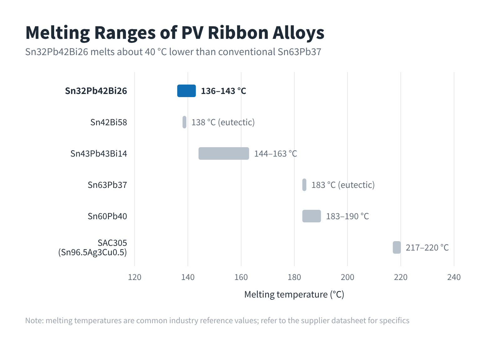
Figure 1 Melting ranges of common PV ribbon alloys
| Alloy | Melting range | Contains lead | Typical positioning |
|---|---|---|---|
| Sn63Pb37 | 183 °C (eutectic) | Yes | Conventional ribbon |
| Sn60Pb40 | ≈ 183–190 °C | Yes | Conventional ribbon |
| Sn43Pb43Bi14 | ≈ 144–163 °C | Yes | Medium/low-temperature ribbon |
| Sn32Pb42Bi26 | ≈ 136–143 °C | Yes | Low-temperature ribbon (focus of this article) |
| Sn42Bi58 | 138 °C (eutectic) | No | Lead-free low-temperature direction |
| SAC305 (Sn96.5Ag3Cu0.5) | ≈ 217–220 °C | No | Mainstream lead-free solder in electronics; melting point too high |
2. Each of the three elements has a job
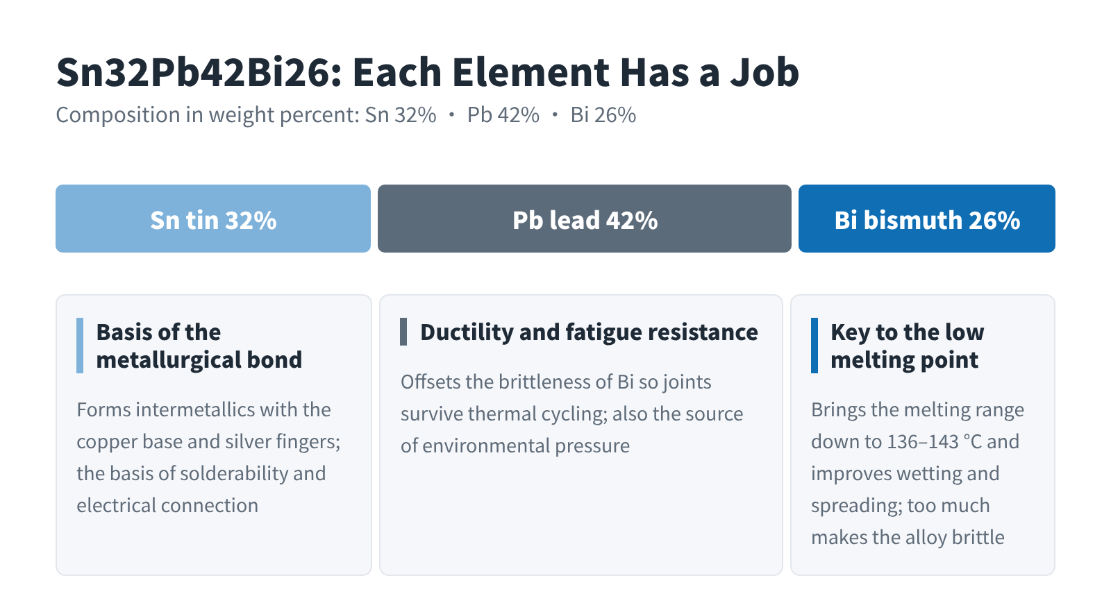
Figure 2 Composition of Sn32Pb42Bi26 and the role of each element
- Bismuth (Bi, 26 %): the key element for lowering the melting point. It also lowers the surface tension of the molten solder, improving spreading and wetting. But Bi itself is rather brittle, so more is not always better.
- Lead (Pb, 42 %): improves ductility and fatigue resistance, offsetting the brittleness from Bi. This is why the alloy is "tougher" than pure Sn-Bi alloys.
- Tin (Sn, 32 %): the main element that forms the metallurgical bond with the copper base and the cells' silver fingers; the basis of solderability and electrical connection.
3. Where it is used
Ribbons in a PV module fall into two groups:
- Interconnect ribbon: connects adjacent cells, carrying current from one cell to the next;
- Bus ribbon: collects the cell strings and leads them to the junction box.
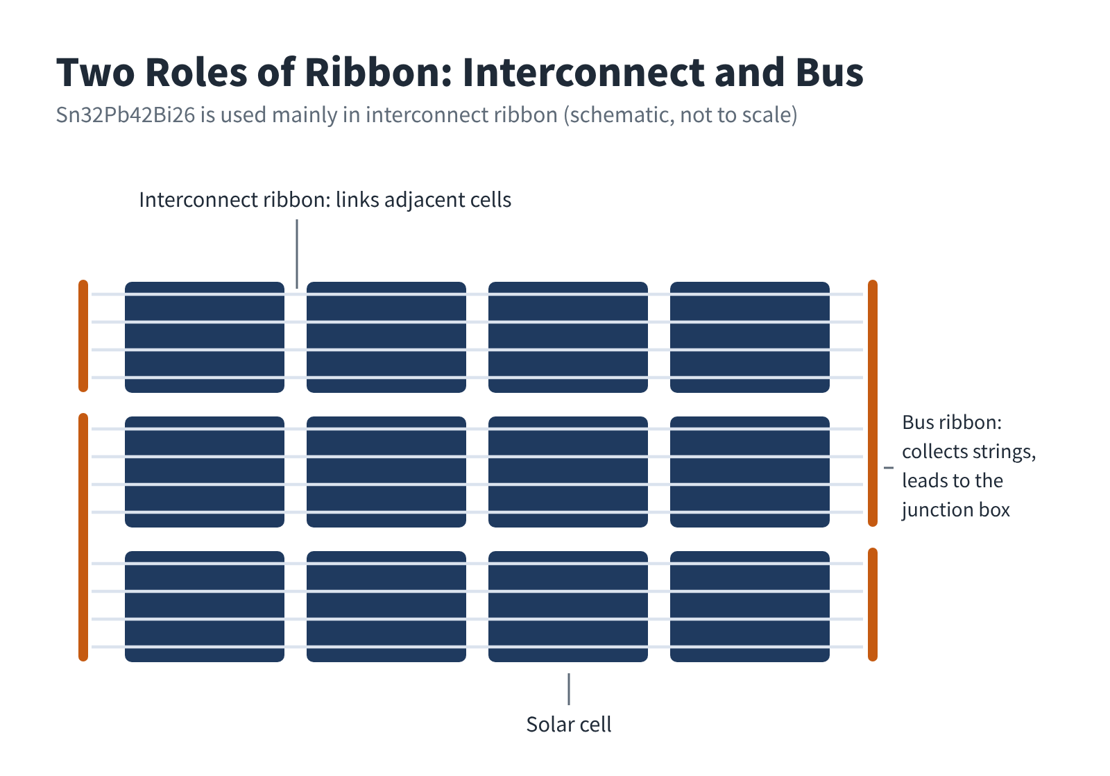
Figure 3 Position of interconnect and bus ribbons in a module (schematic)
Sn32Pb42Bi26 is currently used mainly for interconnect ribbon, and is especially suited to two scenarios (which overlap):
- Lamination soldering in 0BB (zero-busbar) technology: alloying between the ribbon and the fingers happens during lamination, so the solder must melt at around lamination temperature;
- Low-temperature processing in HJT (heterojunction) technology: the amorphous silicon films cannot tolerate high temperatures, so the soldering temperature must be kept low.
The low melting point effectively prevents high-temperature damage to the amorphous silicon layers. According to industry experience data from some manufacturers, it can deliver a module power gain of about 1 %–2 % compared with high-temperature soldering (depending on cell technology and module layout).
03Current status: rapid uptake, but challenges remain
1. Market: growing together with n-type cells
Sn32Pb42Bi26 is in a phase of rapid uptake in PV ribbon, driven mainly by the rise of n-type cells (HJT, TOPCon, etc.).
- A bigger overall market: global PV ribbon demand was about 164,000 t in 2023. Forecasts for 2025 range from 287,000 t to 322,000 t depending on the source (TrendForce EnergyTrend forecast about 273,000 t for 2024 and about 322,000 t for 2025). Interconnect ribbon is used at about 4:1 to 5:1 relative to bus ribbon (about 5:1 for multi-busbar modules).
- Rising share of low-temperature ribbon: according to compiled public data, the share of low-melting ribbons represented by Sn32Pb42Bi26 has risen from under 10 % in 2020 to over 25 % in 2025, mainly on high-efficiency module lines.
- The process works: ribbon with this alloy is compatible with automated stringers and supports soldering speeds of about 4,000 cells per hour.
- Industry structure: China is the world's main production base for PV ribbon, dominated by private companies with low industry concentration. Strong demand for low-melting ribbon from leading module makers keeps shipments of this alloy growing quickly (public sources often cite around 30 % per year).
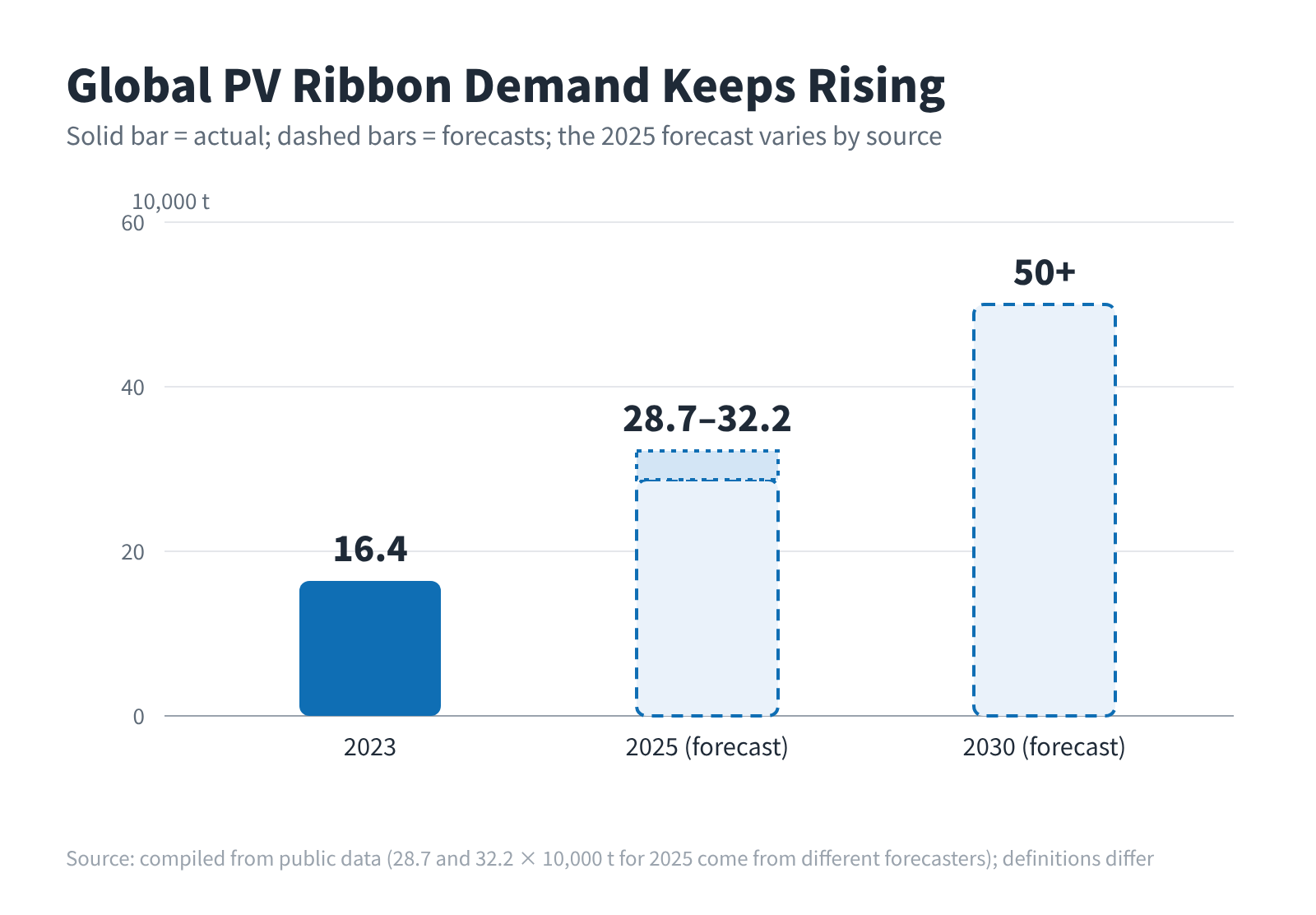
Figure 4 Global PV ribbon demand (2023 actual and later forecasts)
2. Challenges: lead is a compliance issue, bismuth a cost issue
| Challenge | Details |
|---|---|
| High lead content (42 %) | PV panels have been excluded from the scope of the EU RoHS Directive (2011/65/EU) since 2013 and still are. But leaded solder is hard to recycle, and the EU is developing ecodesign-type product requirements for PV modules, with criteria on hazardous substances among the topics under discussion |
| Volatile bismuth prices | According to the U.S. Geological Survey (USGS), bismuth averaged about $5.40/lb in 2024, up about 32 % from 2023. After China imposed export controls on bismuth in February 2025, the monthly average hit $34.22/lb in March; the 2025 annual average is estimated at about $20/lb, roughly four times 2024 and a record high |
Even so, this alloy's penetration in HJT modules has reached about 40 % (public data).
04Outlook: mainstay of the transition, starting point of the shift
1. Demand side: n-type iteration keeps helping
Some institutions forecast that annual global PV installations will exceed 1 TW by 2030, at which point ribbon demand would exceed 500,000 t.
Sn32Pb42Bi26 will keep benefiting from cell technology iteration:
- More low-temperature scenarios: HJT is sensitive to process temperature, 0BB lamination soldering requires alloying around lamination temperature, and BC cells are soldered on one side with high warpage stress. All of these favour lower soldering temperatures;
- Room to go lower: by optimising the Bi content, the melting point could fall further to around 130 °C, improving process compatibility;
- Profiled ribbon adds to the gain: combining this alloy with profiled ribbon (e.g. alternating round-wire and flat segments) reduces shading; figures reported by some manufacturers are about 5 % less shaded area and about 2 % more module power, depending on the module layout.
2. Policy side: environmental pressure is the biggest variable
Environmental regulation is the key factor that will determine this alloy's life cycle. PV panels are still exempt from the EU RoHS Directive, but the EU is advancing ecodesign requirements for PV modules, and hazardous substances are one of the topics under discussion. Once lead restrictions take effect, leaded ribbon will face direct substitution.
The main lead-free low-temperature directions are Sn-Bi and Sn-Bi-Ag alloys. Note that the mainstream lead-free solder in electronics, SAC305 (Sn96.5Ag3Cu0.5), melts at about 217 °C, higher even than conventional tin-lead solder, and is not suitable for low-temperature soldering.
Before going fully lead-free, Sn32Pb42Bi26 can serve as a transition solution: gradually reducing Pb below 20 %, or improving reliability by doping with Ag, Zn and other elements.
Rising bismuth prices hit the lead-free Sn-Bi route harder (Sn42Bi58 contains 58 % bismuth, more than twice this alloy), which in the short term may actually prolong the transition period for leaded low-temperature alloys.
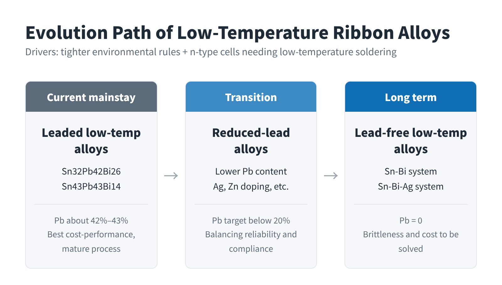
Figure 5 Evolution path of low-temperature PV ribbon alloys
3. Technology and recycling
- Technical innovation: new coatings and AI-optimised soldering parameters could cut overall ribbon cost by about another 10 % and better support shingled and flexible modules;
- Recycling: pyrometallurgical recycling of Pb-Sn-Bi alloys is fairly mature, with metal recovery rates of around 90 %, helping to close the loop. With bismuth prices high, the economics of recycling improve too.
By 2030, the market for ribbon using this alloy is expected to reach the order of RMB 10 billion, with penetration likely to settle at around 30 %. Over a longer horizon, however, reduced-lead and lead-free versions will gradually become mainstream.
05Final thoughts
With its low melting point and good solderability, Sn32Pb42Bi26 has become a key material for low-temperature PV ribbon, helping both to raise module efficiency and to control manufacturing cost.
Today it is growing fast; its future depends on the pace of environmental regulation. Lead is the source of its cost-performance today, and the reason it will be replaced tomorrow. The bismuth price surge since 2025 adds a cost variable to that substitution path.
For practitioners, the task is twofold: seize the window opened by n-type cells and 0BB technology and make the process window and reliability of the current alloy rock-solid; and at the same time start validating reduced-lead and lead-free low-temperature alloys early, while watching bismuth supply and price risk, so as to be ready for the next material switch.
We would be glad to hear about your experience and views on introducing low-temperature ribbon.
References
- U.S. Geological Survey, Mineral Commodity Summaries 2026: Bismuth
- TrendForce EnergyTrend: PV ribbon demand and cost analysis (2024)
- Directive 2011/65/EU (RoHS 2), Article 2(4)(i): exclusion of photovoltaic panels from scope
- PV CYCLE: Photovoltaic waste legislation details (RoHS exemption and ecodesign for PV panels)
A PV R&D and technology team with 10+ years of experience | In-depth technical knowledge sharing
Materials · Reliability · Failure Analysis · Standards & Certification · Products · Processes
Exploring AI + PV; collaboration welcome
Disclaimer:
1. Original content reflects the authors' personal views only, is for reference only and does not constitute investment advice.
2. Reposted and cited content is credited to its source, out of respect for original work.
3. Some content was produced with AI assistance (chart generation, data retrieval, concept explanations, etc.); the core framework and key content were written by our technical team and reviewed by people.
4. If anything is inaccurate or infringes your rights, please leave a message or contact us and we will deal with it.