
A 1.95 eV Perovskite Hits 16.5% Certified — How Should We Read “Passing IEC 61215 at the Cell Level”?
01What is a 1.95 eV perovskite for?
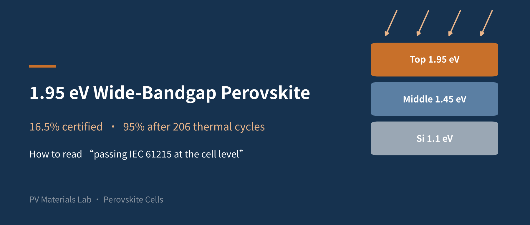
A perovskite’s bandgap can be tuned through its halide ratio. The ideal single-junction bandgap is around 1.3–1.4 eV, and top cells for perovskite/silicon tandems usually sit at 1.65–1.70 eV. The 1.9–2.0 eV range is mainly for the top cell of a triple-junction stack. One study estimates that adding 1.45 eV and 1.95 eV perovskite layers on a silicon bottom cell could push the theoretical triple-junction efficiency above 35% [3].
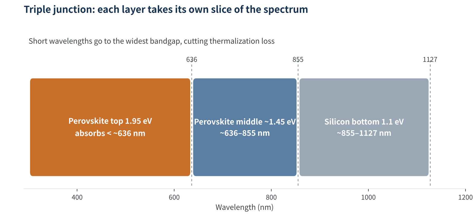
Figure 1 How the sub-cells of a triple-junction stack split the spectrum (cut-off wavelength ≈ 1240/Eg)
The difficulty: the wider the bandgap, the more bromide is needed, and under light the iodide and bromide ions tend to cluster separately, forming small iodide-rich, lower-bandgap regions. This is light-induced phase segregation (the Hoke effect). The iodide-rich regions funnel carriers, capping the open-circuit voltage and hurting long-term stability. A 2023 Nature paper noted that segregation is especially severe in triple-junction top cells, which need an absorber of about 2.0 eV [2]. That is why 1.95 eV cells are generally not very efficient — the mid-teens already counts as a good result.
02What the paper did
I-BDC is a small molecule with an iodine atom on the benzene ring of isophthalic acid. Its two carboxyl groups can coordinate with under-coordinated Pb²⁺ in the film, passivating defects. The authors report that it also suppresses phase segregation: films containing I-BDC showed stable photoluminescence (PL) over 120 minutes of illumination. The key data disclosed in the abstract are summarized below.
Table 1 Key data from the paper (source: abstract)
| Item | Reported | Our note |
|---|---|---|
| Bandgap | 1.95 eV | Triple-junction top-cell range |
| Certified PCE | 16.5% (reverse scan) | Lab and area not disclosed |
| Film photostability | Stable PL over 120 min light | Film level, short duration |
| MPP tracking | ~40 °C, 500 h, 90% retained | Encapsulated device |
| Thermal cycling | −40↔85 °C, 206 cycles, 95% retained | A second encapsulated device |
| IEC claim | “Passing IEC 61215 protocols at the cell level” | No module-level data |
03How to read the three numbers
- 16.5% certified: Genuinely strong for this bandgap, with two caveats. First, it is a reverse-scan value; perovskites show hysteresis, reverse scans usually read high, and the tandem field cares more about steady-state efficiency. Second, the certifying lab and active area are not given in the abstract, and 0.1 cm²-class and 1 cm²-class results are not directly comparable.
- MPPT 500 h at 90%: The right method, but about 40 °C is a mild test temperature. High-temperature light-soaking protocols in the ISOS consensus typically use 65 °C or 85 °C [4], and outdoor modules often operate above 60 °C.
- 206 thermal cycles at 95%: The temperature range matches IEC 61215 thermal cycling and the cycle count slightly exceeds 200 — the most “engineering-grade” number in the paper. But 95% retention means a 5% loss, right on the 5% pass line commonly used in module tests, so the margin is thin.
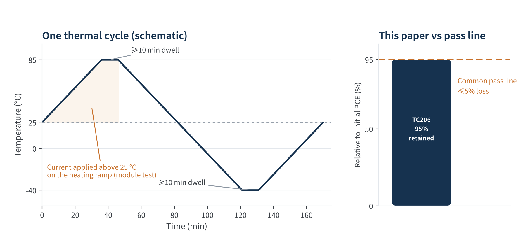
Figure 2 One IEC 61215 thermal cycle (schematic) and the paper’s result
04The limits of “passing IEC 61215 at the cell level”
IEC 61215 is the design qualification and type approval standard for terrestrial PV modules. Its test object is the module, and the verdict rests on a full test sequence; the standard has no notion of a “cell-level pass” [5]. What the authors mean is closer to “we tested an encapsulated cell under IEC 61215 thermal cycling conditions and it stayed within the pass criterion”. That statement is fine in itself, but it is easily shortened to “IEC certified”, which is a very different claim. The differences come in four forms:
- Different structure: Module thermal cycling failures come mainly from ribbon/interconnect fatigue, solder joint cracking and encapsulant delamination — all rooted in mismatched thermal expansion [6]. A small encapsulated cell has no ribbons, no large glass sheet and no frame, so most of that stress is simply absent.
- Different loading: In IEC thermal cycling, modules carry a current close to their peak-power current during the heating ramp, mimicking combined electrical and thermal stress in daytime operation. The abstract does not say whether the cell-level test was biased.
- Different scope: Thermal cycling is just one item in the 61215 sequence. Damp heat (DH1000), humidity-freeze, UV preconditioning and mechanical load — the stresses perovskites are most sensitive to — do not appear in the abstract.
- Unknown encapsulation: Small-device thermal cycling results depend heavily on the package — glass/glass with edge seal, or a simple cover. The abstract does not say, so extrapolating to modules is risky.
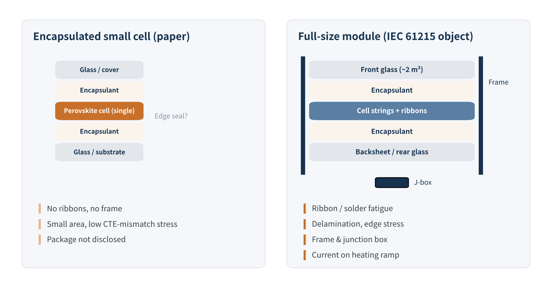
Figure 3 Stresses seen by an encapsulated small cell vs a full-size module during thermal cycling
Perovskites also show reversible degradation and light-soaking recovery, so how devices are stabilized and when they are measured can change the “retention” figure. The ISOS consensus specifically recommends reporting these details [4].
These thermal cycling data show that the I-BDC system, in the authors’ package, does not fall apart under thermal shock — a good sign. But this is a material/device-level screening result, not a module reliability conclusion.
05The bigger triple-junction picture
Wide-bandgap top cells are one of the bottlenecks of the triple-junction route. For reference: in 2024 a KIT-led team reached 24.4% with a perovskite/perovskite/silicon triple junction using a ~1.84 eV top cell [8]; a 2023 Nature paper reported an all-perovskite triple junction with a ~2.0 eV inorganic top cell and 23.3% certified efficiency [2]; and in 2025 a University of Sydney team built a 16 cm² triple-junction cell with a 1.91 eV top cell, certified at 23.3% steady-state, and completed thermal cycling tests [7].
Top-cell bandgaps are moving toward the ideal 1.9–2.0 eV, and stability is the sticking point. Additive strategies are simple and cheap and can be grafted onto other recipes; the value of this paper is that it reports certified efficiency and thermal cycling numbers together. How I-BDC performs inside a triple-junction device, and whether it stays uniform and effective in large-area coating, still awaits further data.
06Final thoughts
This is a wide-bandgap top-cell materials paper worth watching: 16.5% certified efficiency and 206 thermal cycles show the direction is right, but “passing IEC 61215 at the cell level” does not mean module reliability is proven — a full test sequence still lies between this and product-level qualification.
When you next see “passes IEC” in a perovskite paper, we suggest asking three questions:
- What was tested: a cell, a mini-module, or a full-size module?
- Which tests: thermal cycling only, or also damp heat, humidity-freeze, UV and mechanical load?
- How was it packaged and measured: what encapsulation, was it biased, and how was it stabilized before measurement?
We will keep tracking reliability progress in perovskite tandems, and we welcome comments from colleagues working on encapsulation and certification.
Data for this paper come from the ACS Energy Letters abstract (public Crossref record); the full text and supporting information were not available to us. “Not disclosed” means not mentioned in the abstract — the full text may provide it. Data for other work come from their papers or public reports; device areas and structures differ, so they are for directional reference only, not direct comparison. Cut-off wavelengths are converted as λ ≈ 1240/Eg (nm).
References
- Tao R. et al. ACS Energy Letters, 2026 (online; I-BDC-stabilized 1.95 eV wide-bandgap perovskite). DOI: 10.1021/acsenergylett.6c01702 (abstract)
- Wang Z. et al. Suppressed phase segregation for triple-junction perovskite solar cells. Nature, 2023, 618: 74–79.
- High-Bandgap Perovskite Materials for Multijunction Solar Cells. Joule, 2018 (Perspective).
- Khenkin M. V. et al. Consensus statement for stability assessment and reporting for perovskite photovoltaics based on ISOS procedures. Nature Energy, 2020, 5: 35–49.
- IEC 61215-1 / IEC 61215-2. Terrestrial photovoltaic (PV) modules – Design qualification and type approval.
- Kiwa PVEL. PV Module Product Qualification Program: Thermal Cycling.
- Physics World. Large-area triple-junction perovskite solar cell achieves record efficiency, Oct 2025 (University of Sydney, Nature Nanotechnology).
- KIT et al. Triple-junction perovskite–perovskite–silicon solar cells with power conversion efficiency of 24.4%. Energy & Environmental Science, 2024.
PV Materials Lab
A PV R&D and technology team with 10+ years of experience | In-depth technical knowledge sharing
Materials · Reliability · Failure Analysis · Standards & Certification · Products · Processes
Exploring AI + PV — collaboration welcome
Disclaimer:
1. Original content reflects the author’s personal views, is for reference only, and does not constitute investment advice.
2. Reproduced and cited content is attributed to its source, with respect for original work.
3. Some content is AI-assisted (chart generation, data retrieval, concept explanations, etc.); the core framework and key content are written by our technical team and reviewed by humans.
4. For any inaccuracy or infringement, please leave a comment or contact us.