
The Lifesaver in the Junction Box: PV Bypass Diodes Explained
130, 150, 180, trench, planar... what are PV engineers actually talking about?
A bypass diode is a negligible share of a module's cost, yet it guards the module's safety. This article explains what it does, why almost all are Schottky diodes and which datasheet parameters matter, and translates jargon like "130 trench" and "180 planar" into plain language.
Turn a PV module over and you will see one (or three) small black boxes: the junction box. It is the "exit" through which the module delivers current, and the real stars inside are a few chips smaller than a mung bean: bypass diodes.
They are a negligible part of a module's cost, yet they guard its safety. In this article we explain them in plain language, and decode what PV people mean when they talk about a "130 trench" or a "180 planar".
01What it does: an emergency lane for current
The cells in a module are connected in series, one after another, like a single-lane road: current must pass through every cell in turn.
Here is the problem. If one cell is covered by a leaf, bird droppings, dust or a shadow from the row in front, it cannot generate as much current, yet the other cells still "push" current through it. It is no longer a source but a reverse-biased load, turning power from the other cells into heat. This is a hot spot: at best it causes power loss; at worst it burns through the backsheet, shatters glass or even starts a fire.
The fix is to connect a diode in parallel with each string of cells:
- In normal operation: the diode is reverse-biased and "off", consuming almost nothing;
- When a cell is shaded: the voltage across that string reverses, the diode turns on automatically, and current goes around through it.
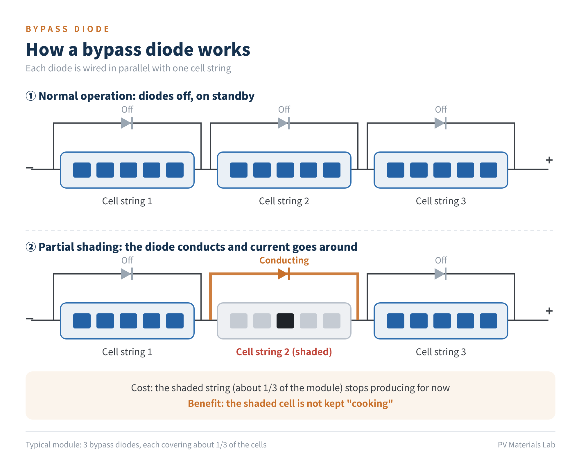
Figure 1 How a bypass diode works
A typical module has three bypass diodes, each covering about a third of the cells. So if a leaf covers one cell, the worst outcome is that this third goes "offline" for a while, instead of dragging down the whole module or the whole string.
① A bypass diode is not a blocking diode. A blocking (anti-reverse) diode sits in series in the circuit to stop reverse current; it serves a different purpose.
② Bypass diodes do not eliminate hot spots. They only cap the reverse voltage across a shaded cell at "the voltage of one substring". The risk is capped, not removed.
02Why they are almost all Schottky diodes
When a diode conducts, it has a forward voltage drop VF, so current flowing through it produces heat:
Heat dissipated ≈ forward voltage VF × current
- Ordinary silicon PN junction diode: VF about 0.7–1 V;
- Schottky diode: VF about 0.4–0.5 V.
Today's large-format modules easily carry more than 15 A. Do the maths: 15 A × 0.45 V ≈ 7 W. Don't underestimate those 7 W: they are generated inside a small, sealed, potted box stuck to the back of a module baking in the sun. With a PN diode it would be well over 10 W, which the box could hardly withstand. That is why low-VF Schottky diodes became the industry standard.
But Schottky diodes have "character flaws": high reverse leakage current, which is very temperature-sensitive; a limited reverse voltage rating; and sensitivity to electrostatic discharge and lightning surges. The debates over parameters and processes discussed below mostly revolve around this pair of rivals: forward voltage and leakage.
03Reading the datasheet: six key parameters
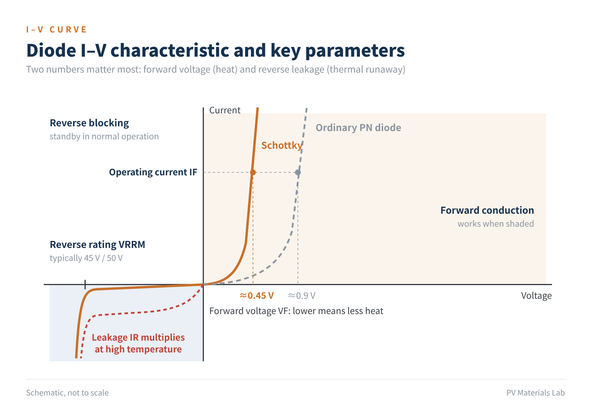
Figure 2 Diode I–V characteristic and key parameters (schematic)
| Parameter | In plain terms | What to look for |
|---|---|---|
| VRRM reverse voltage | Reverse voltage it can withstand when off | Usually 45 V / 50 V; a substring's open-circuit voltage is only a dozen or so volts, so the margin is ample |
| IF rated forward current | Current it can carry continuously | Diodes are often rated 30 / 40 / 50 A; note this is not the junction box rating |
| VF forward voltage | The "toll" paid when conducting | Lower is better; it directly sets the heat |
| IR reverse leakage | Current that sneaks through when off | Tiny at room temperature, multiplies at high temperature; the root of thermal runaway |
| Tj max junction temperature | Highest temperature the chip can tolerate | PV Schottky diodes are commonly rated around 200 °C; check the datasheet |
| Rth thermal resistance | How easily heat leaves the chip | Set by the package and box design; lower is better |
The 30 A or 50 A on a diode datasheet is given under fairly ideal cooling. Once mounted in a junction box, potted, and stuck to a module back at 70–80 °C, the current it can safely carry is derated.
Public junction box datasheets often show pairings like this: a diode rated 50 A / 45 V, with a box rated 30 A. So for junction boxes, look at the rated current of the whole box.
Two "big exams"
Bypass diode thermal test (IEC 61215-2, MQT 18.1): heat the module to 75 °C, pass a current equal to the module's short-circuit current Isc through the diode and determine the junction temperature; then raise it to 1.25 × Isc for one hour. The junction temperature must not exceed the diode's rated maximum, and the diode must still work after the test (MQT 18.2 functionality check).
Two changes in the current edition, IEC 61215-2:2021, are worth noting. First, not every diode needs to be tested; three are selected. Second, test methods for bifacial modules were added, so test currents for bifacial modules must account for rear-side gain. This ties directly to the rising module currents discussed later.
Thermal runaway test (IEC 62979): specific to Schottky diodes. The diode is first "soaked" with forward current at high temperature, then quickly switched to reverse voltage to see whether it can cool down on its own.
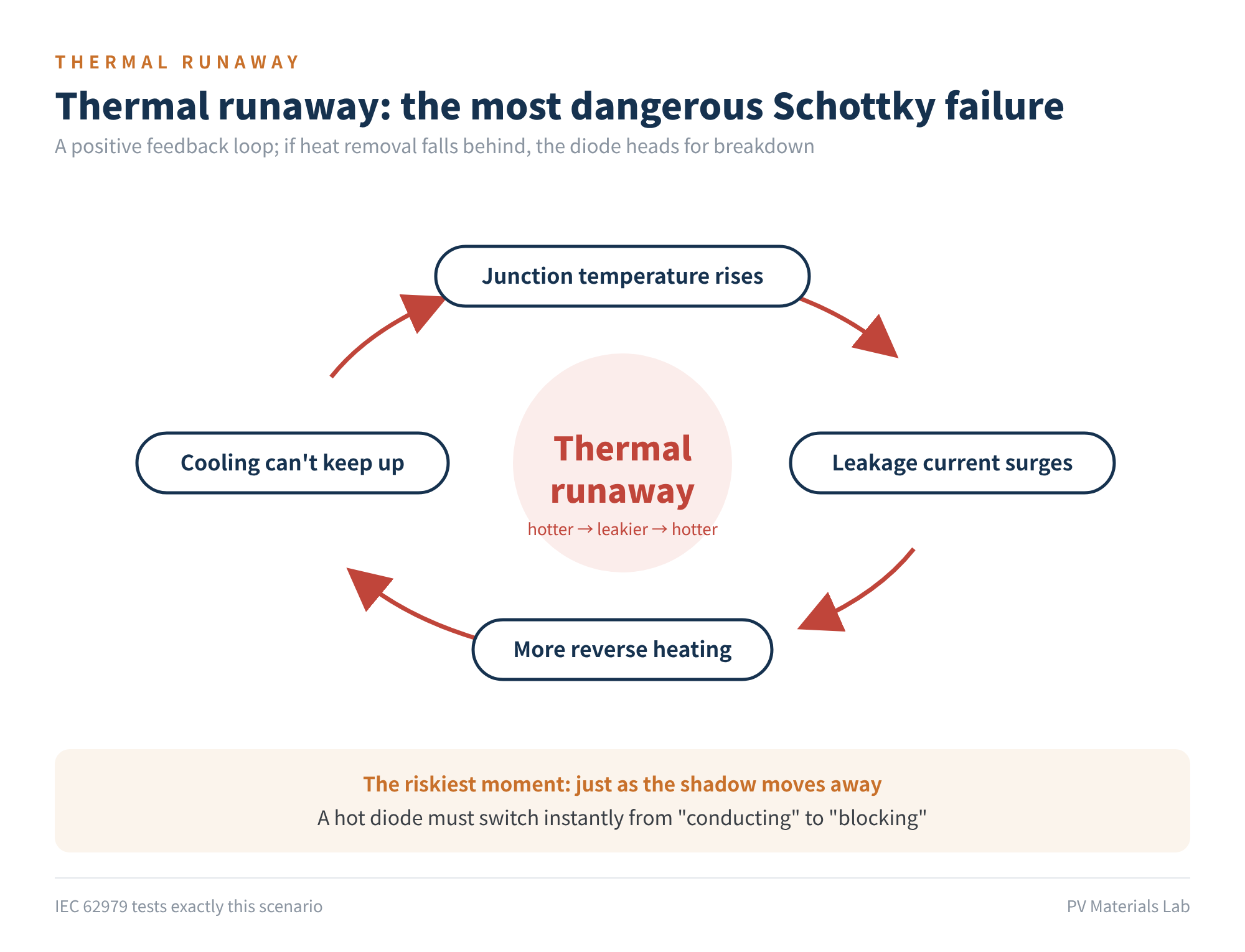
Figure 3 Thermal runaway: the most dangerous Schottky failure mode
Thermal runaway is a positive feedback loop: the hotter the diode, the higher the leakage; the higher the leakage, the more reverse heating; the more heating, the hotter it gets... If cooling cannot keep up, it heads all the way to breakdown and short circuit, and in severe cases burns out the junction box.
04Jargon decoded: 130, 150, 180, planar, trench
"This box uses a 150 trench." "Can we switch to a 130 to cut cost?" Conversations like these are common in purchasing negotiations and technical reviews. Broken down, they are about two things:
The number = how big the chip is | The word = how the chip is made
The number: chip side length, in mil
The mil is an imperial unit still used in the semiconductor industry: 1 mil = 1/1000 inch = 0.0254 mm. Diode chips are square, and "150" means a chip with a side length of 150 mil.
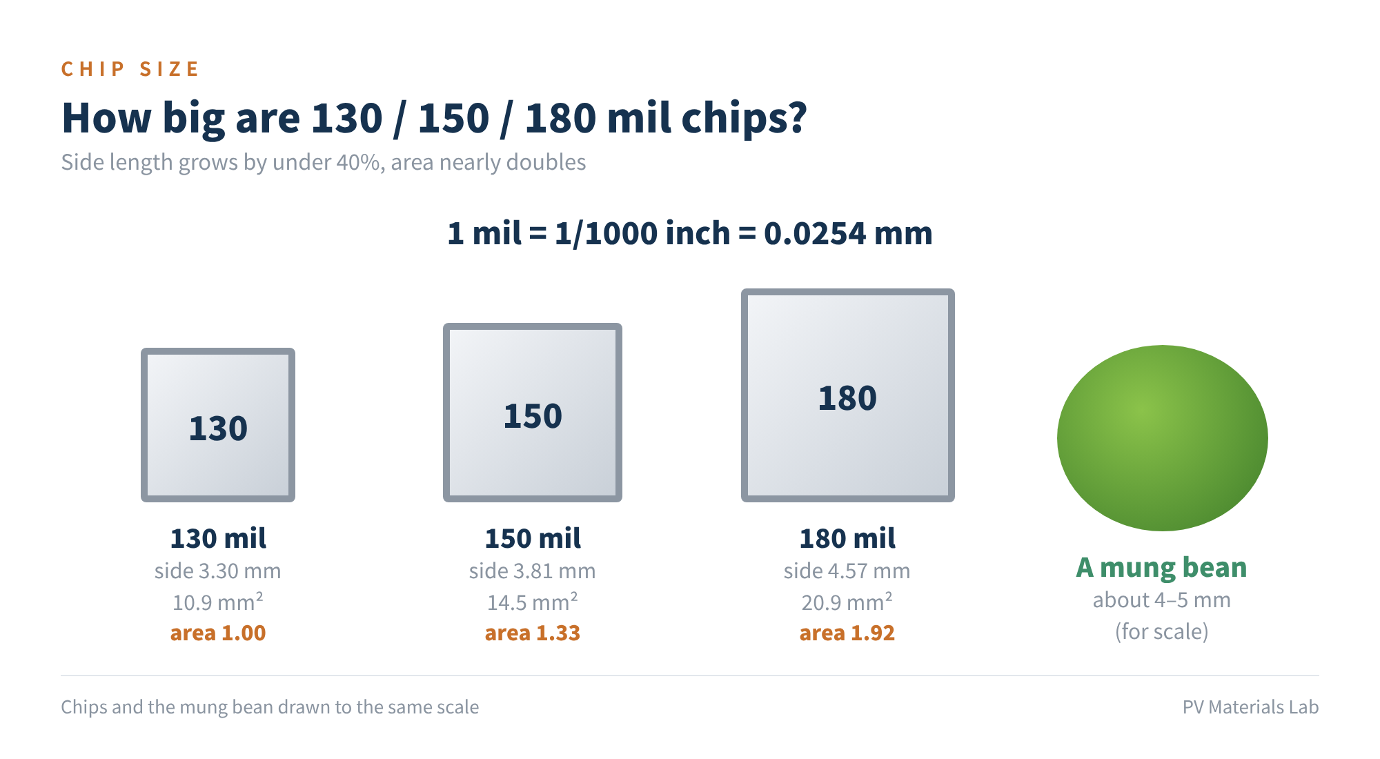
Figure 4 Actual size of 130 / 150 / 180 mil chips
| Name | Side | Area | Relative area |
|---|---|---|---|
| 130 | 3.30 mm | 10.9 mm² | 1.00 |
| 150 | 3.81 mm | 14.5 mm² | 1.33 |
| 180 | 4.57 mm | 20.9 mm² | 1.92 |
Note that area grows with the square: the 180's side is less than 40% longer than the 130's, but its area is nearly double.
What does a bigger chip buy you? The same current spread over a larger area means lower current density, so lower forward voltage and less heat; the larger contact area with the copper also lets heat escape more easily. So the higher the module current, the bigger the chip usually is.
The cost is just as direct: silicon is paid for by area, so bigger chips cost more, and leakage also rises roughly with area. Choosing a chip size is essentially a trade-off between safety margin and cost, which is exactly why it keeps coming up.
Planar / trench: two internal structures
The heart of a Schottky diode is a metal–silicon contact (the Schottky barrier).
- Planar: the contact is flat. The structure is simple, the process mature and the cost low. Its difficulty is a "seesaw": push the forward voltage down and leakage multiplies; hold leakage down and the forward voltage won't drop.
- Trench: rows of micron-scale deep trenches are etched into the silicon surface, an oxide layer is grown on the walls, and the trenches are filled. Under reverse bias, adjacent trenches "pinch off" the silicon between them like two doors closing, shielding the metal–silicon interface from the strong field and holding leakage down. That headroom lets the forward voltage be made lower.
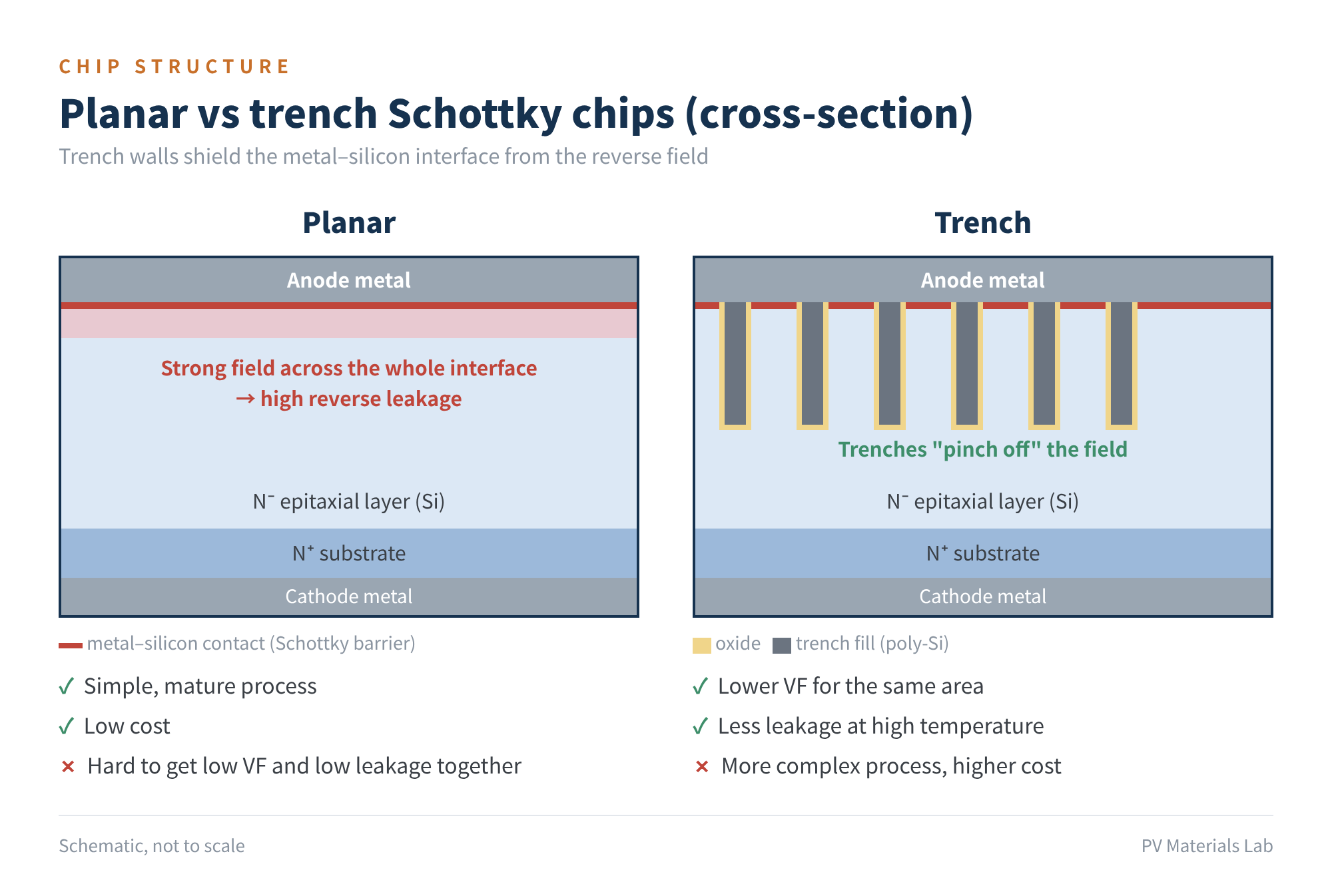
Figure 5 Cross-section of planar and trench Schottky chips (schematic)
| Item | Planar | Trench |
|---|---|---|
| Forward voltage | Higher | Lower |
| High-temperature leakage | Larger | Smaller |
| Thermal runaway resistance | Average | Better |
| Process and cost | Simple, cheap | Complex, somewhat pricier |
| Chip size for the same current | Larger | Can be smaller |
Put the two together:
- "150 trench": a trench Schottky chip with 150 mil sides;
- "180 planar": a planar Schottky chip with 180 mil sides.
Because trench chips "punch above their weight" per unit area, the industry often pits a trench chip one size smaller against a planar chip one size larger. But whether one can replace the other ultimately depends on measured junction temperature and thermal runaway data in the specific junction box, not on the numbers alone.
A few more terms
- 3045 / 4045 / 5045: numbers in common diode part names; the first two digits are current (A), the last two are voltage (V). 5045 means 50 A / 45 V.
- Axial / SMD / module: the three package types of diode (see Figure 6).
- One-piece / split box: three diodes in one box, or three small boxes with one diode each.
- Potting: filling the box with thermally conductive sealant, which waterproofs it and helps dissipate heat.
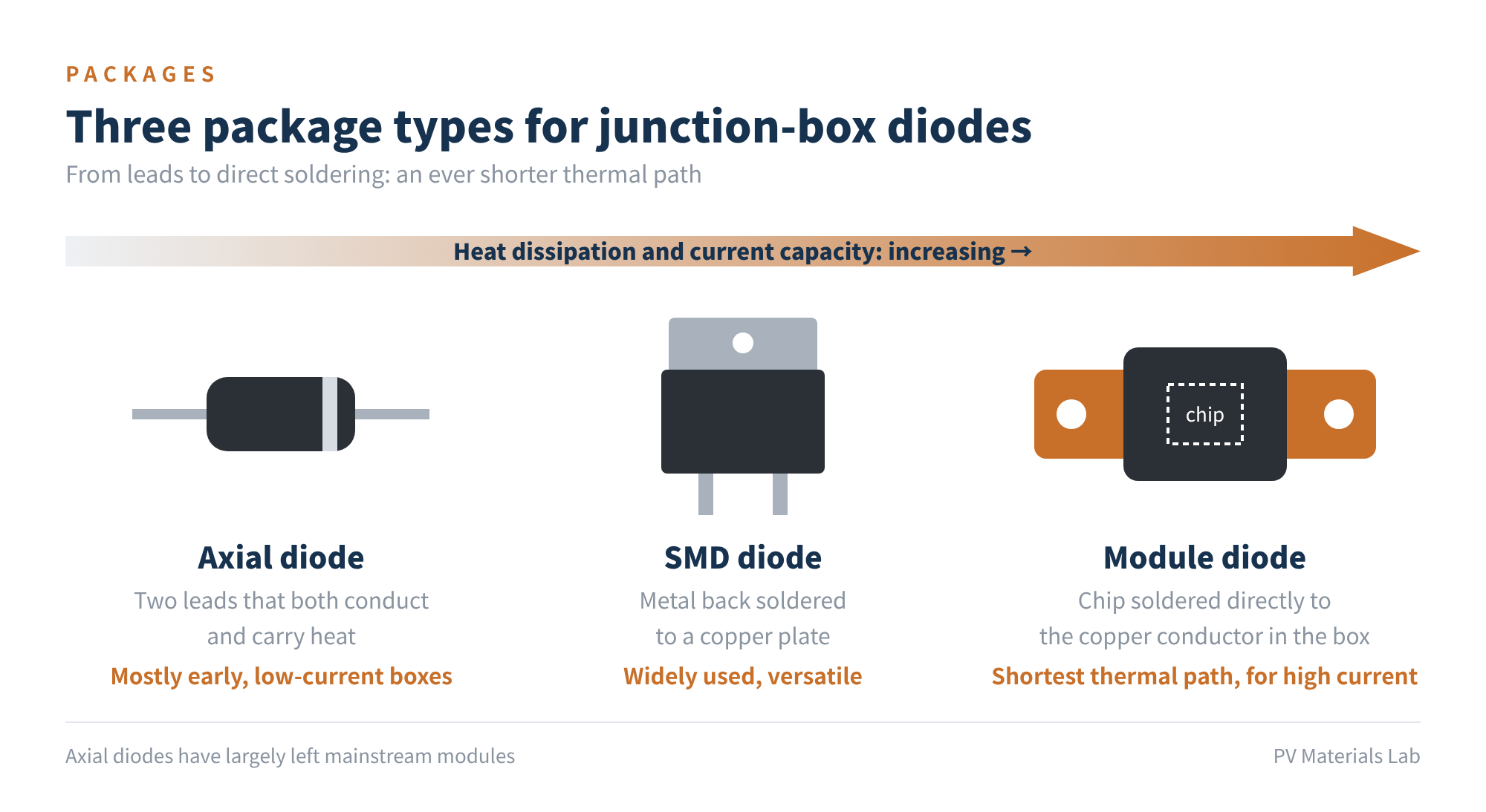
Figure 6 Three package types for junction-box diodes
05Production today: what "standard" looks like in the high-current era
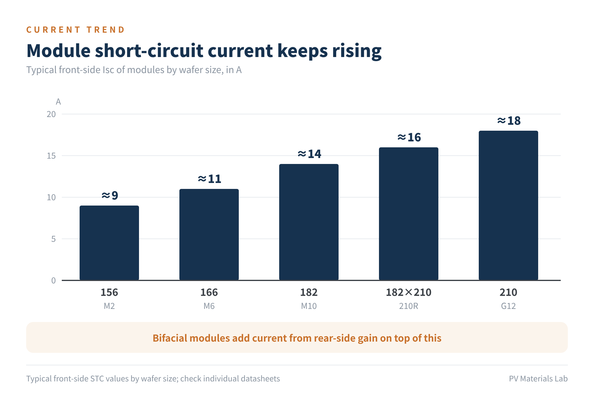
Figure 7 Module short-circuit current keeps rising with wafer size (typical values)
Over the past few years, wafers have grown from 156 to 182 and 210 mm, and module short-circuit current has risen from about 9 A to 14–18 A, with rear-side gain from bifacial modules on top. A recent example: a 210R (182×210) 66-cell TOPCon bifacial module whose datasheet is dated January 2026 lists a front-side Isc of 16.27 A for its 640 W class and a maximum series fuse of 35 A. Doubling the current more than doubles the challenge for the diode. Production today looks roughly like this:
- Box type: split, potted junction boxes dominate. Three small boxes each hold one diode, spreading out the heat sources, which also suits half-cell module layouts.
- Package: axial diodes have largely left mainstream modules; SMD and module diodes coexist. Module diodes solder the chip directly to the copper conductor in the box and then encapsulate it, giving the shortest thermal path; they are increasingly used in high-current products. In 2023 the China Photovoltaic Industry Association published a group standard specifically for them, T/CPIA 0052—2023, Module diodes for PV module junction boxes.
- Current ratings: whole-box ratings are mainly 25 A and 30 A, extending to 35 A, 40 A and above, for 210 and high-power bifacial modules.
- Chips: planar and trench coexist, and trench keeps gaining share in high-current products; chip sizes are moving up overall, with 130, 150 and 180 all common.
- Supply chain: highly localised in China. Junction box makers include Tonglin, QC Solar (Kuaike) and Zerun, and diode and chip suppliers include Yangjie Technology and Good-Ark (Suzhou Gude).
The other side is worth mentioning too: junction boxes are among the module BOM categories under the most cost-down pressure. A chip one size smaller, thinner copper, less potting... each step eats into the safety margin. As module currents grow while boxes get leaner, diode selection deserves ever more careful attention.
06Looking ahead: how diodes will change
- Higher current, lower forward voltage. As module power keeps rising, bigger chips, wider use of trench processes and continued improvement of box thermal design are the most certain directions.
- Active bypass, or "ideal diodes". A MOSFET plus control circuit replaces the Schottky, with a conduction drop of just tens of millivolts. Take Texas Instruments' SM74611: TI quotes an average forward drop of about 26 mV at 8 A and typical dissipation of about 0.2 W, against about 3.2 W for a conventional Schottky under the same conditions. That is an order of magnitude less heat, without Schottky's high-temperature leakage. The barriers are cost, proving the reliability of electronics outdoors for over 20 years, and current rating: this chip's maximum operating current is 15 A, already short of today's 16–18 A high-current modules.
- Smart junction boxes. Integrating optimisers, rapid shutdown and monitoring/communication into the junction box turns the diode from a stand-alone part into part of a power-electronics system. The opportunity is bigger in distributed PV and in markets with regulatory requirements for safety shutdown.
- A variable from cell technology. Some new cells (such as certain BC cells) have a low reverse breakdown voltage, so when shaded the cell itself "soft-conducts" at a low voltage, easing hot-spot risk. In global BC field data released in December 2025, LONGi also stated that its Hi-MO 9 effectively suppresses the hot-spot effect under partial shading from vegetation, bird droppings and dust (no specific temperature figures were given). This will change how bypass protection is designed, but for now the diode remains an indispensable safety baseline.
- Stricter standards and validation. Conditions such as thermal runaway, high current and bifacial gain are increasingly being written into test standards and technical agreements.
07Final thoughts
The bypass diode is the kind of part you never notice until something goes wrong. Three points are all you need to remember:
Its job: make way for current when shaded, putting a cap on hot-spot risk.
The core trade-off in selection: forward voltage (heat) versus leakage (thermal runaway).
Two pieces of jargon: "130 / 150 / 180" is about chip size; "planar / trench" is about chip structure. Bigger and trench usually mean more safety margin, and also higher cost.
What diode issues have you run into in selection or failure analysis? We would be glad to hear from you.
References
- IEC 61215-2:2021, Terrestrial photovoltaic (PV) modules – Design qualification and type approval – Part 2: Test procedures (MQT 18 bypass diode tests)
- IEC 62790:2020, Junction boxes for photovoltaic modules – Safety requirements and tests (2nd edition)
- IEC 62979:2017, Photovoltaic modules – Bypass diode – Thermal runaway test
- T/CPIA 0052—2023, Module diodes for PV module junction boxes (China Photovoltaic Industry Association group standard)
- Texas Instruments: SM74611 Smart Bypass Diode product page
- Renew: G12R TOPCon module datasheet, January 2026
- LONGi: "LONGi Releases Global BC Technology Field Data", 2 December 2025
A PV R&D and technology team with 10+ years of experience | In-depth technical knowledge sharing
Materials · Reliability · Failure Analysis · Standards & Certification · Products · Processes
Exploring AI + PV; collaboration welcome
Disclaimer:
1. Original content reflects the authors' personal views only, is for reference only and does not constitute investment advice.
2. Reposted and cited content is credited to its source, out of respect for original work.
3. Some content was produced with AI assistance (chart generation, data retrieval, concept explanations, etc.); the core framework and key content were written by our technical team and reviewed by people.
4. If anything is inaccurate or infringes your rights, please leave a message or contact us and we will deal with it.