
After 0.16 mm: How Much Thinner Can 0BB Round Ribbon Go?
Key points
Publicly verifiable mass production of 0BB ribbon is mainly 0.18–0.20 mm, with 0.16 mm the thinnest size today. Below that, resistance, pull force and alignment windows all tighten. Using a set of simplified calculations, we estimate the application limit of round ribbon in modules.
A human hair is about 0.07 mm across. The thinnest 0BB ribbons used in PV modules today are 0.16 mm, only a little thicker than two hairs side by side. In a module more than two metres long, over a thousand such fine copper wires carry the current out cell by cell.
Everyone knows ribbons keep getting thinner. But can they keep going? How much room is left below 0.16 mm? This article first verifies today's mass-production sizes, then uses a few simple physical relationships to estimate the application limit of round ribbon in modules.
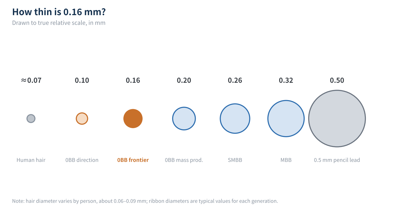
Figure 1 Ribbon diameters by generation, to true scale against a hair and a pencil lead
01Meet the 0BB ribbon
0BB stands for zero busbar. A conventional cell front has two kinds of silver lines: dense fingers collect current, and busbars at right angles to them gather it, with ribbons soldered onto the busbars. In 0BB, the cell has no printed busbars, and in the module the ribbon contacts the fingers directly, doing both the collecting and the series connection.
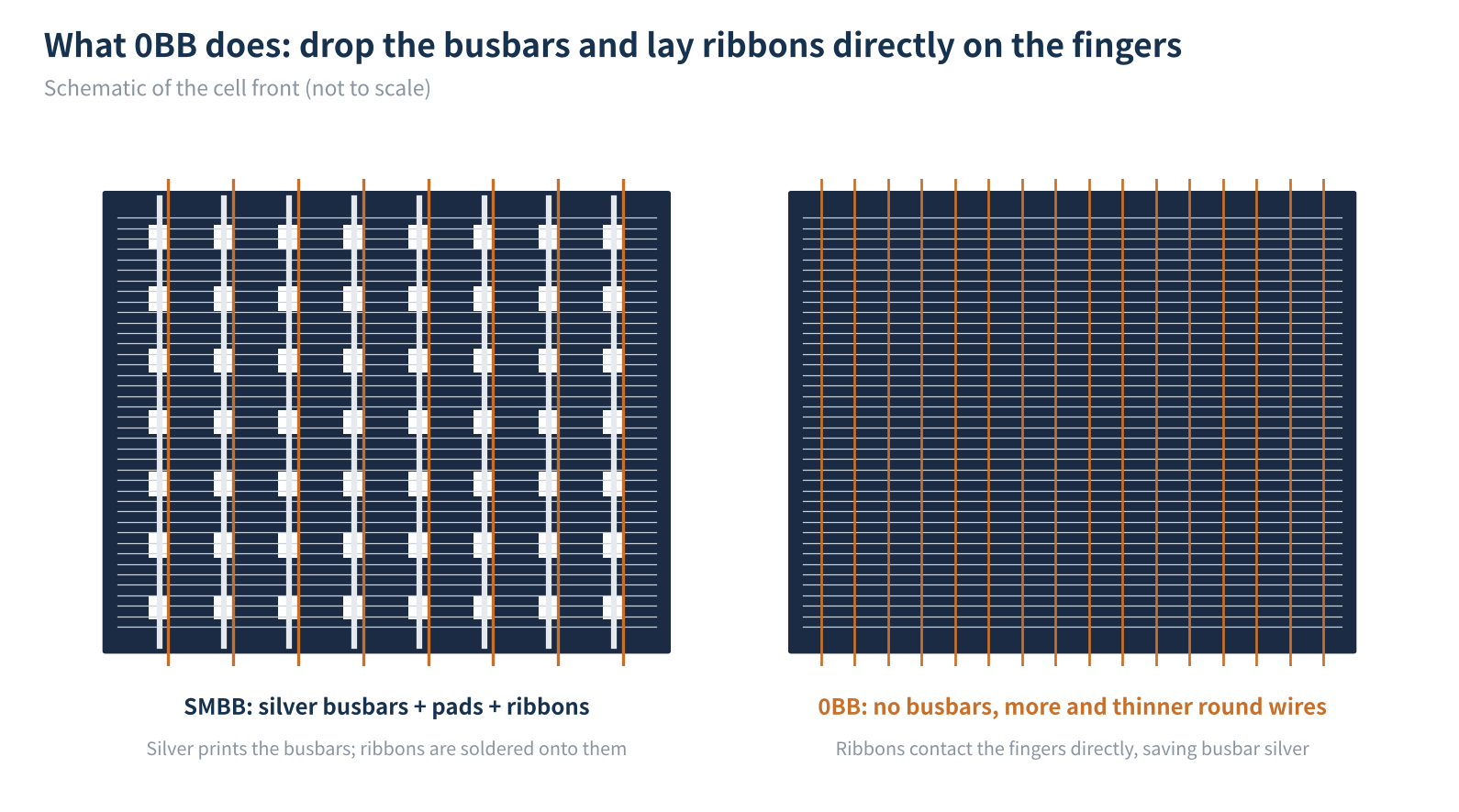
Figure 2 Front of SMBB and 0BB cells (schematic)
Removing the busbars saves silver paste. On broker research estimates, silver paste consumption can fall by 10%–20% for TOPCon and about 30% for HJT. The higher the silver price, the better the economics, which is the main reason 0BB has spread quickly from HJT to TOPCon and BC over the past two years.
The economics became more pressing after 2025. According to a TMTPost review in January 2026, the London spot silver price rose about 147% over 2025, ending the year at about USD 71.6/oz, and silver paste's share of module cost rose from about 10.5% in January 2024 to 16%–17% in January 2026. Silver-reduction routes such as 0BB, finer finger printing, silver-coated copper and copper plating have all accelerated as a result. These routes are not mutually exclusive: on copper-plated cells, for example, 0BB is also used to ease warping caused by interconnection heating.
The 0BB ribbon itself is simple in structure: an annealed soft copper wire inside, with a solder alloy coating outside. The difficulty is that it must be thinner, softer and more evenly coated than earlier ribbons, and where alloying is completed during lamination, it must also switch to lower-melting solders containing bismuth or indium.
02How thin is mass production really?
Answers online vary, so we put the publicly available sources in order:
- Definition: Tongxiang Technology's 2024 interim report describes 0BB ribbon as tin-coated ribbon with a diameter ≤ 0.22 mm; Zhongyuan Securities' industry report at the end of 2024 likewise defines it as "ultra-fine round ribbon of 0.22 mm and below".
- Mass production: at the TaiyangNews high-efficiency technology conference at the end of 2024, a leading Chinese ribbon maker said ultra-low-temperature ribbons of 0.18 mm and 0.20 mm diameter were in industrial mass production. A 2024 Soochow Securities report said leading makers' 0BB ribbons were 0.18–0.22 mm.
- Trend: a market research summary from June 2026 said 0BB ribbon diameters are "generally ≤ 0.20 mm" and listed ≤ 0.18 mm as the next iteration.
- Lower bound: a Zhonglai Optoelectronics patent on 0BB modules gives a preferred round wire diameter of 0.16–0.22 mm; 0.16 mm is the thinnest application size appearing in public sources.
Public sources confirm 0.18–0.20 mm as mainstream mass production; 0.16 mm is at the leading edge and the thinnest size in the public domain today.
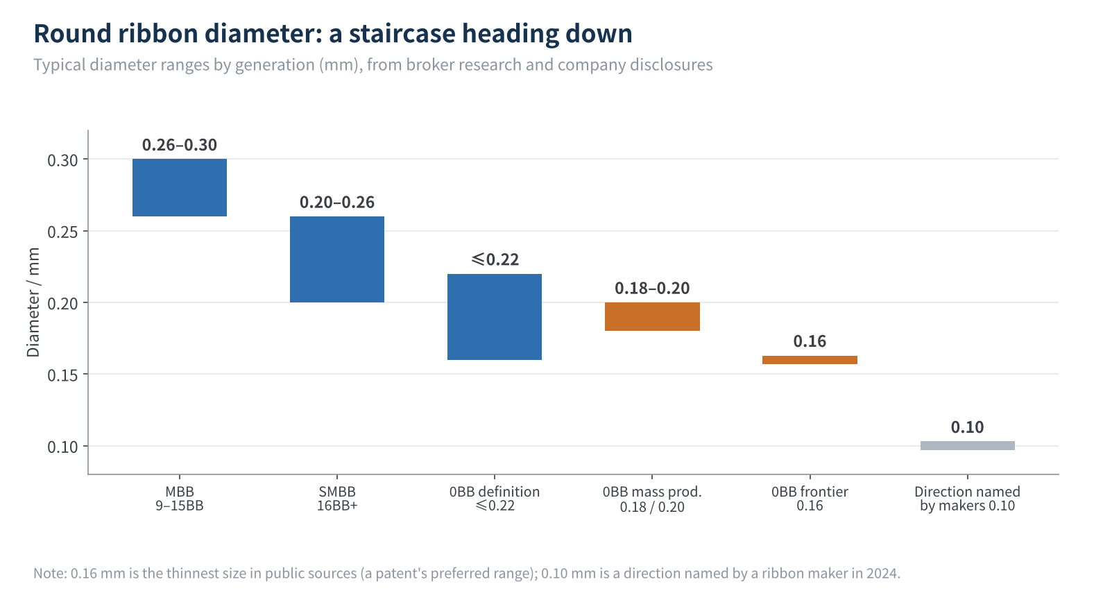
Figure 3 Evolution of round ribbon diameter
Two more numbers are worth noting. As early as 2022, broker research mentioned that leading ribbon makers could already reach 0.14 mm in the lab; in November 2024, a Yubang New Material executive told Cailian Press that round ribbon diameters "will move further towards 0.10 mm in future". In other words, drawing the wire thinner is not the problem. The electronics industry has long made enamelled wire and bonding wire below 0.05 mm. The question is whether wire this fine still pays off, and stays reliable, in a module.
03Why go thinner?
Thinner wires bring four main benefits:
- Less shading. The ribbon sits on the cell front and blocks light. The smaller the diameter, the less area it covers.
- Supporting silver reduction. The more ribbons, the shorter the path current must travel along the fingers, so fingers can be printed narrower and thinner. With more ribbons, each must be thinner, or shading and cost become unacceptable.
- Lower stress, suited to thin wafers. Thin, soft copper wire puts less thermal stress on the cell, keeping crack risk manageable as wafers go to 110 μm and below.
- Less encapsulant, copper and tin. Thinner ribbons mean a lower step for the encapsulant to fill, so its weight can drop. Copper per ribbon scales with diameter squared: 0.16 mm weighs only 64% as much per metre as 0.20 mm.
It all looks like good news. But every benefit comes with a bill to pay.
04The first bill: resistance
A conductor's resistance is inversely proportional to its cross-section, which scales with diameter squared. So going from 0.20 mm to 0.16 mm cuts the diameter by only 20%, but cuts the cross-section by 36% and raises resistance per metre by about 60%.
There is also an easily overlooked factor: the coating. Solder has about 8 times the resistivity of copper and contributes almost nothing to conduction, but to ensure soldering, the coating cannot shrink in proportion with the diameter. Assuming 12 μm per side, copper makes up 77% of the cross-section of a 0.20 mm ribbon but only 58% at 0.10 mm.
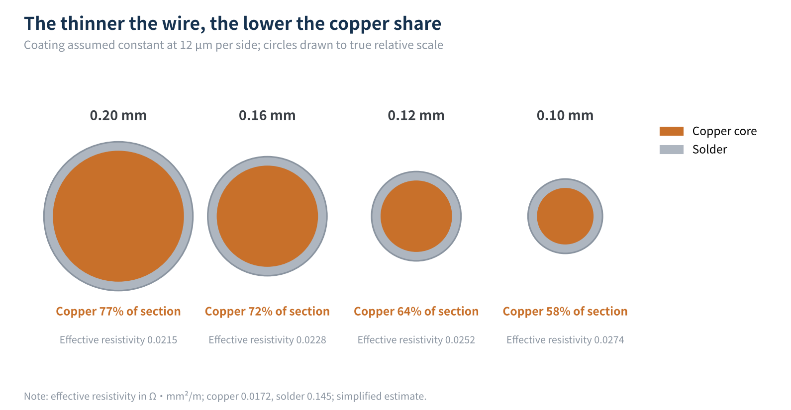
Figure 4 Copper core share of the cross-section by diameter (coating 12 μm per side)
Combining the two factors gives this comparison table:
| Diameter mm | Resistance per metre Ω | Ribbons needed for equal loss | Yield force N |
|---|---|---|---|
| 0.20 | 0.68 | 1.00× | 3.14 |
| 0.18 | 0.87 | 1.27× | 2.54 |
| 0.16 | 1.13 | 1.66× | 2.01 |
| 0.14 | 1.54 | 2.26× | 1.54 |
| 0.12 | 2.23 | 3.26× | 1.13 |
| 0.10 | 3.49 | 5.11× | 0.79 |
Table 1 Resistance and pull force by ribbon diameter (simplified estimate, yield strength 100 MPa)
The third column shows how many times more ribbons are needed to keep ribbon ohmic loss unchanged: 1.66× for 0.16 mm, more than 3× for 0.12 mm, and 5× for 0.10 mm.
This rule has in fact held throughout the past decade. Roughly checking typical combinations by generation (9BB with 0.35 mm, 12BB with 0.32 mm, 16BB with 0.27 mm, 20BB with 0.23 mm), "number of ribbons × diameter squared" has always stayed between 1.05 and 1.25. Every time the industry made ribbons thinner, it made up the total conducting cross-section by adding more ribbons.
What if the number of ribbons stays the same? We estimated a 210R format with 24 ribbons per cell:
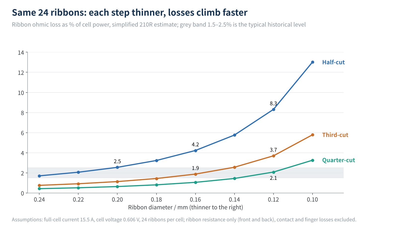
Figure 5 Ribbon ohmic loss versus diameter with 24 ribbons (simplified estimate)
On a half-cut cell, ohmic loss with 0.20 mm ribbon is about 2.5%; switching to 0.16 mm raises it to about 4.2%, 1.7 percentage points more. Meanwhile geometric shading only falls from 2.6% to 2.1%, a 0.5-point gain, and since round wire reflects some light back onto the cell, the real shading gain is smaller still. Switching to thinner wire without adding ribbons loses power.
The other two lines show the way out: cut the cells smaller. A third-cut cell carries two-thirds of the half-cell current over two-thirds of the path, so ribbon loss falls to 44% of the half-cell value; a quarter-cut cell falls to 25%. With third-cut cells, 0.16 mm returns to 1.9% loss; 0.12 mm needs quarter-cut cells to get back to around 2%.
05The second bill: pull force, alignment and soldering
Beyond resistance there are three process constraints.
- It can't be pulled hard. 0BB ribbon uses annealed soft copper with a yield strength around 100 MPa. Yield force is about 3.1 N for 0.20 mm ribbon, about 2.0 N for 0.16 mm, and only about 0.8 N for 0.10 mm, the weight of an 80-gram mass. Stringers pull dozens of ribbons at high speed; with any tension fluctuation, the fine wire stretches thinner and its resistance rises further.
- It won't lie straight. The bending stiffness of a round wire scales with diameter to the fourth power. At 0.16 mm stiffness is only 41% of 0.20 mm, and at 0.10 mm just 6%: as limp as thread and hard to keep straight. Ribbon makers have reported in public that even 0.20 mm ribbon shows drift in 0BB processes, mitigated by raising yield strength and applying about 2% pre-stretch. But higher yield strength means harder copper and more stress on the cell, which contradicts the very purpose of going thinner.
- It's hard to bond well. 0BB ribbon rests directly on fingers only twenty to thirty microns wide, so each crossing has a small contact area to begin with. The thinner the wire, the less solder, and the closer the contact gets to a single point, making contact resistance and peel force harder to guarantee. Coating concentricity is also harder to control: the same 3 μm offset barely matters for 0.20 mm ribbon but can leave one side of a 0.10 mm ribbon clearly short of solder.
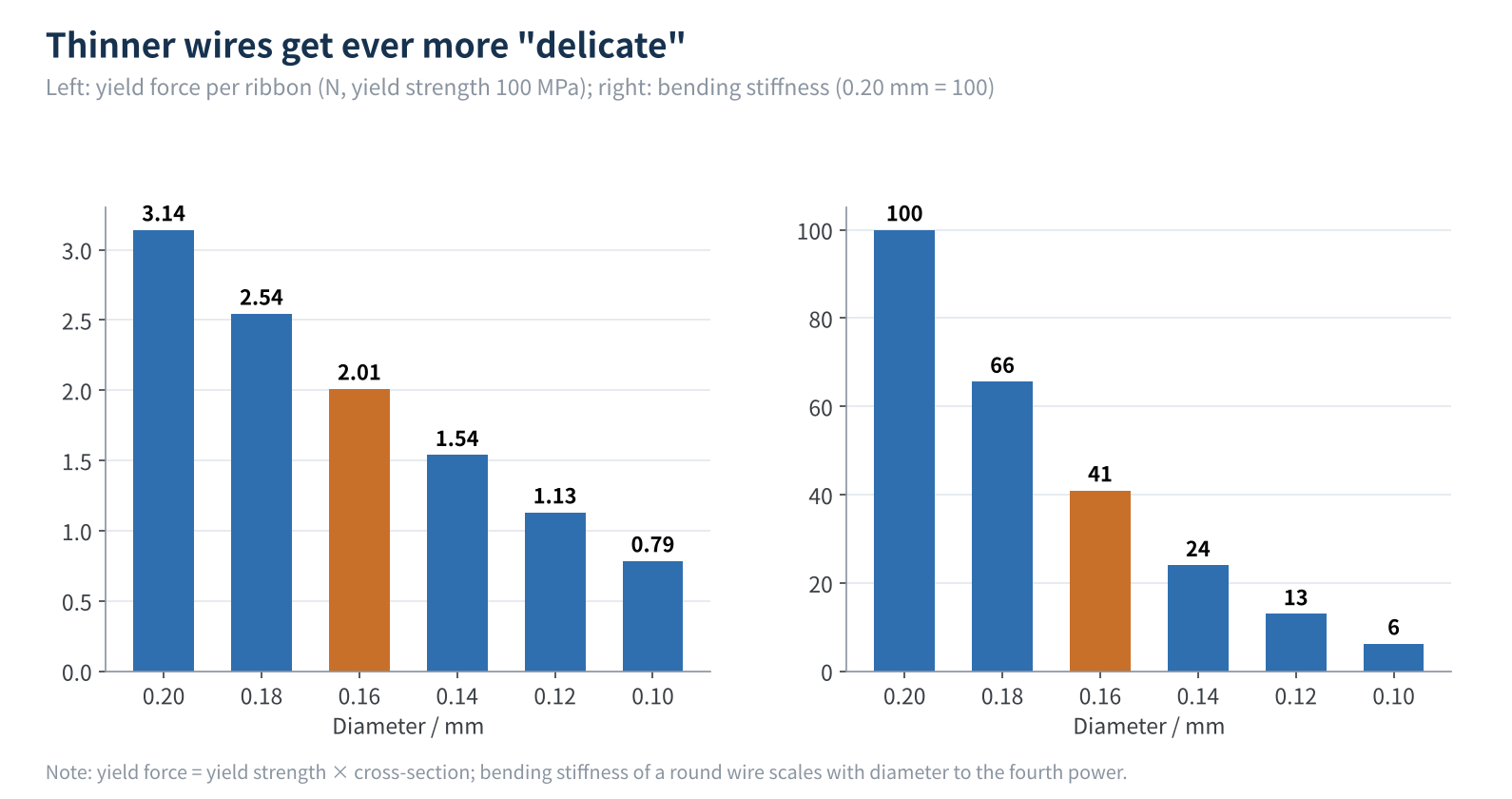
Figure 6 Effect of diameter on yield force and bending stiffness
06So where is the limit?
Putting these constraints together gives a stage-by-stage judgement. Note that this is an estimate based on a simplified model, not an industry consensus.
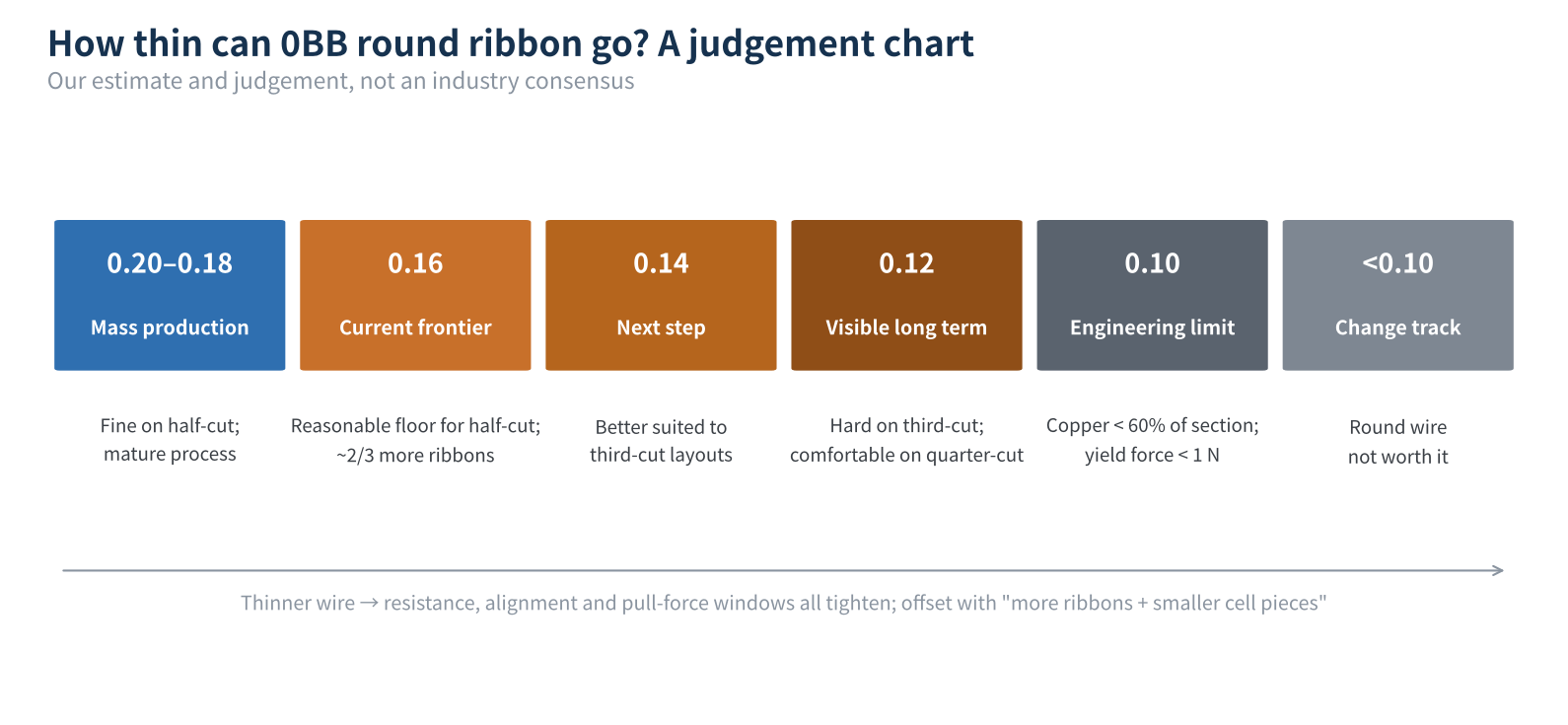
Figure 7 Stage-by-stage judgement on thinning 0BB round ribbon
- 0.18–0.20 mm: comfortable in resistance and process on half-cut layouts; the mass-production mainstream confirmed by public sources.
- 0.16 mm: already close to the reasonable floor for half-cut layouts. Keeping losses in check needs about two-thirds more ribbons than at 0.20 mm, a clear step up in stringer wiring density and tension control.
- 0.14 mm: technically feasible, but hard to justify on half-cut cells; better suited to third-cut layouts.
- 0.12 mm: a struggle even on third-cut cells; comfortable only on quarter-cut. And the more pieces a cell is cut into, the greater the cost in cutting loss, cell spacing and stringer takt time.
- 0.10 mm: can be seen as the engineering limit for round ribbon in modules. Copper is less than 60% of the section, yield force per ribbon is under 1 N, and every constraint is pushed to the edge.
- Below 0.10 mm: continuing with round wire isn't worth it. A change of approach is more likely, such as shaped ribbons, conductive adhesive interconnection, or changing the metallisation scheme at the cell itself.
From today's 0.16 mm, 0BB round ribbon has roughly "two small steps" left: first to 0.14 mm, then to 0.12 mm, with 0.10 mm as the visible end point. How fast it gets there depends not on whether ribbon makers can draw finer wire, but on whether module makers are willing to cut smaller pieces and lay denser wires.
07Final thoughts
Ribbon thinning is not a metric that can be optimised on its own. Each step down in diameter requires ribbon count, cell cutting, stringer equipment, encapsulant and solder formulation to be adjusted together. Seen this way, whether 0.16 mm becomes mainstream and when 0.14 mm appears is really a system question: how high silver prices are, how thin wafers get, and how fast the equipment cost of multi-cut layouts falls.
We will keep tracking actual ribbon diameters on production lines. How do you pair ribbon diameter and count on your lines? We would be glad to hear from you.
References
- Tongxiang (Suzhou) Electronic Materials Technology Co., Ltd., 2024 interim report
- Zhongyuan Securities, power equipment and new energy industry 0BB report, December 2024
- TaiyangNews: Ribbons For 0BB Metallization, 28 January 2025
- Soochow Securities: "0BB helps TOPCon cut costs and raise efficiency, poised to scale up", June 2024
- Tianfeng Securities: "0BB report 2: a key competitive point in new PV technology; 2024 may be the year of industrialisation", May 2024
- Dongxing Securities, 0BB industry research report, July 2024
- Broker initiation report on Tongxiang Technology, December 2022
- Cailian Press: "Yubang New Material: multilayer composite PV ribbon in volume use; Anhui project about to start production", November 2024
- Taizhou Zhonglai Optoelectronics Technology Co., Ltd., patent CN217788408U
- Taoyue Consulting: "0BB PV ribbon in rapid growth, supporting a new cycle of PV cost reduction and efficiency gains", June 2026
- TMTPost: "From 'silicon is king' to 'silver reduction is king': who will win the next PV cycle?", 5 January 2026
A PV R&D and technology team with 10+ years of experience | In-depth technical knowledge sharing
Materials · Reliability · Failure Analysis · Standards & Certification · Products · Processes
Exploring AI + PV; collaboration welcome
Disclaimer:
1. Original content reflects the authors' personal views only, is for reference only and does not constitute investment advice.
2. Reposted and cited content is credited to its source, out of respect for original work.
3. Some content was produced with AI assistance (chart generation, data retrieval, concept explanations, etc.); the core framework and key content were written by our technical team and reviewed by people.
4. If anything is inaccurate or infringes your rights, please leave a message or contact us and we will deal with it.