
Common Ribbon-Related Failures: From Dark EL Cells to Cracked Solder Joints
In brief
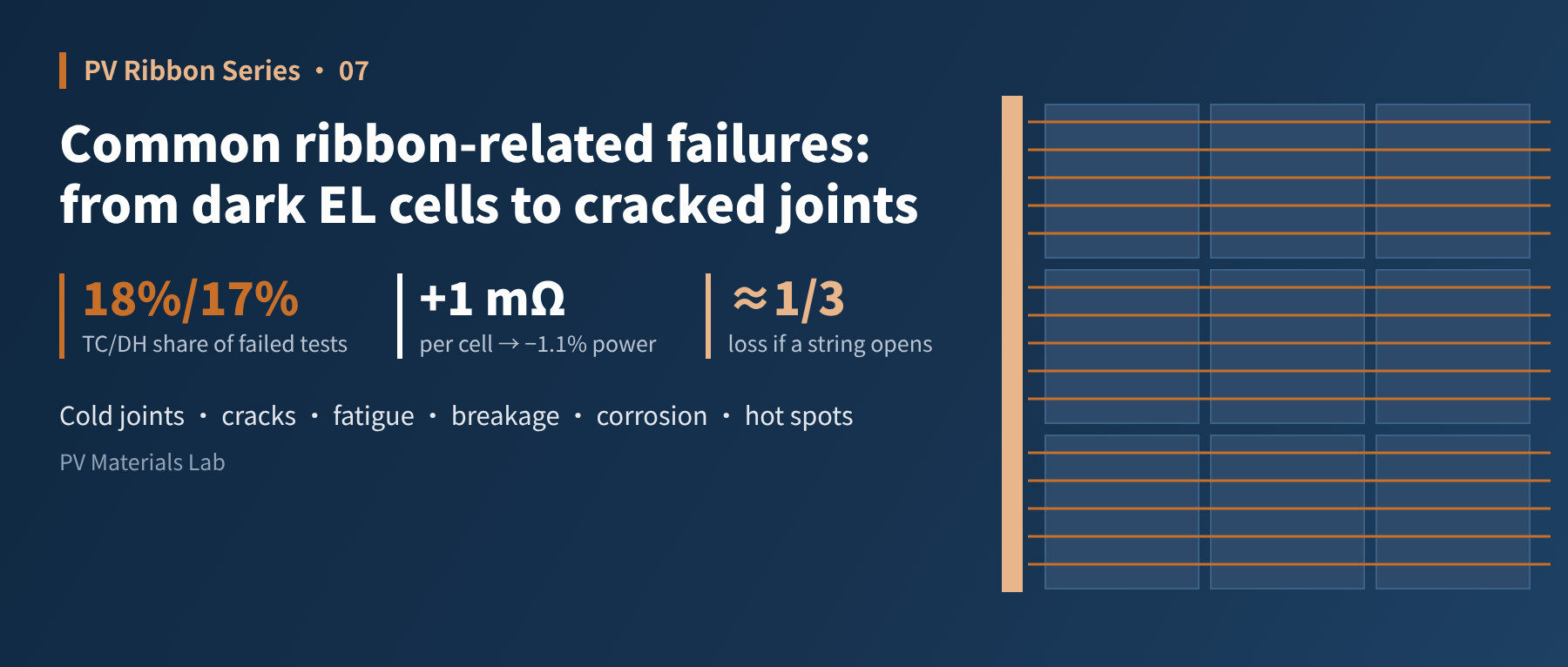
Ribbon-related failures span the whole module life: cold joints and micro-cracks in manufacturing, then solder joint fatigue, interconnect ribbon breakage, corrosion and hot spots in the field. This article follows that timeline to set out how each failure appears, its mechanism and its consequences, draws on IEA PVPS failure reports and solder ageing research, estimates how rising series resistance affects power, and closes with a failure analysis approach that works from symptom to root cause.
In the previous articles we covered how ribbon is selected, made, tested and soldered. This article takes a different angle: what does it look like when things go wrong? In module failure analysis, ribbon-related problems are very common, and they often have a long "incubation period": EL looks fine at the factory, and the problem only emerges slowly years later. Here we follow the module's life cycle and take apart the common ribbon-related failures one by one.
01A failure map
Ribbon-related failures can be roughly grouped into three categories by when they occur:
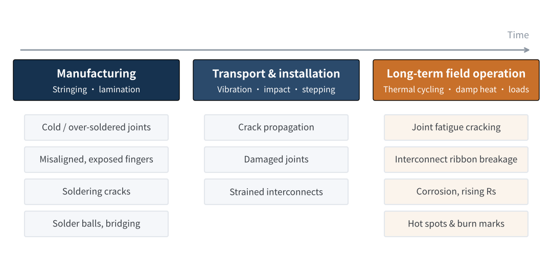
Figure 1 Ribbon-related failures by life-cycle stage (schematic)
How common are these problems? The Review of Failures of Photovoltaic Modules (2014) published by IEA PVPS (the International Energy Agency's Photovoltaic Power Systems Programme) Task 13 gives several data points:
- Early customer complaints: in complaint statistics covering about 2 million modules from a German distributor during the first two years after delivery, "cell interconnect defects" ranked among the main failure types, together with junction box failure, glass breakage, loose frames and delamination.
- Certification testing: across about 1,740 crystalline silicon certification projects, thermal cycling (TC200) accounted for about 18% of failed tests and damp heat (DH) for about 17%, and these are precisely the tests that stress solder joints and ribbon.
- Burn marks in the field: in a study of modules from 21 manufacturers after 8 years in operation, burn marks on cells made up about 10% of all failures. Such burn marks are usually linked to local overheating of interconnect ribbon, solder joints or busbars.
Clearly, ribbon and solder joints are among the parts of a module most likely to "go wrong" over the long term. We now go through them in chronological order.
02Manufacturing: cold joints, over-soldering and soldering cracks
Most manufacturing problems can be found by EL inspection. In the previous article we discussed the soldering temperature window; manufacturing defects are essentially problems on "either side of the window":
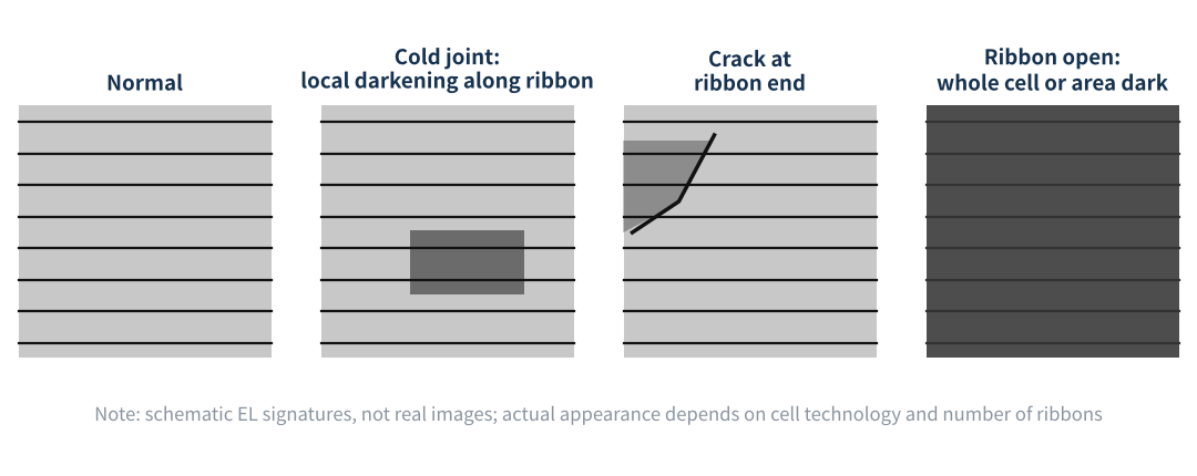
Figure 2 Typical EL signatures of several ribbon-related defects (schematic)
- Cold joints: the solder has not fully wetted the metallisation and the joint merely "sits" on it. EL often shows local darkening along the ribbon. With many ribbons in the multi-busbar era, the effect of one ribbon's cold joints is spread out, so the EL signature is less obvious than before and easier to miss.
- Over-soldering: too high a temperature or too long a time damages the metallisation and passivation around the joint; in severe cases the joint yellows and local cell efficiency drops.
- Soldering cracks: typically at the ribbon ends and near joints. The ribbon end is a stress concentration point, and copper shrinkage on cooling "pulls" cracks into the cell edge. EL shows linear dark lines starting from the ribbon end, or dark areas isolated by cracks.
- Misaligned soldering, exposed fingers: the ribbon is off the metallisation, so the soldered area is too small and fingers are shaded, affecting both peel force and current collection.
The real danger of manufacturing defects is not the immediate power loss but that they become the "starting point" of field failures. A joint with low initial peel force cracks earlier under thermal cycling; a small micro-crack keeps growing under transport, installation, wind and snow loads, and eventually forms a failed area.
It is worth noting that multi-busbar technology has also changed the consequences of cracks. The IEA PVPS Task 13 report on degradation and failure modes in new technologies, published in February 2025, concludes that the impact of cell cracking "has been mostly overcome by the innovation of multi-wire technology": with many closely spaced ribbons, areas isolated by cracks can still deliver current to a nearby ribbon. That does not mean cracks can be ignored; they remain potential starting points for later failures of joints and interconnect ribbons.
Most manufacturing-stage ribbon defects are visible in EL, but multi-busbar designs make cold joints harder to see and reduce the power impact of cracks. Manufacturing defects still deserve "zero tolerance", because they are the seeds of field failures.
03Solder joint fatigue: one "bend" a day
Outdoors, a module goes through one temperature cycle every day: module temperature can reach 60–70 °C during the day and falls back to ambient at night. As we calculated in the previous article, the thermal expansion difference between copper and silicon produces mismatch strain far beyond copper's elastic range. So every day each joint undergoes one cycle of "pull and push".
This cyclic deformation gradually accumulates damage inside the joint:
- Solder creep and microstructure coarsening: tin-lead and similar solders creep even near room temperature; repeated deformation gradually coarsens and segregates the phase structure inside the solder, lowering its strength.
- IMC growth: the intermetallic compounds between solder and copper or silver slowly thicken with temperature and time. IMC is hard and brittle, and the thicker it is, the more easily it cracks along the interface.
- Crack initiation and growth: cracks usually start at the joint edge or the IMC interface and gradually grow inward, reducing the effective conducting area and raising series resistance.
A team from Arizona State University and NREL (IEEE Journal of Photovoltaics, 2020) studied solder joint ageing in two sets of modules that had operated outdoors in Arizona for 21 and 18 years, with useful conclusions: for joints with silver-containing Sn62Pb36Ag2 solder, the activation energy for solder bond degradation was about 0.12 eV, versus about 0.35 eV for silver-free Sn60Pb40, so the former is less temperature-sensitive; IMC thickness in both increased with module temperature, and the silver-free joints showed marked phase segregation in all temperature zones. The study concludes that silver in the solder helps mitigate solder bond degradation.
The direct consequence of joint fatigue is rising series resistance. Let's estimate its effect on power:
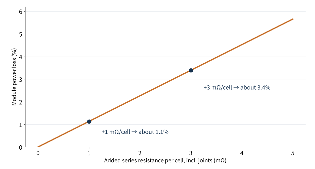
Figure 3 Effect of added series resistance per cell on module power (estimate)
For a 144 half-cell module of about 580 W, if series resistance per cell (including joints) rises by 1 mΩ on average, module power falls by about 1.1%; at 3 mΩ, by about 3.4%. How much is 1 mΩ? A 0.26 mm copper round wire has about 0.33 mΩ/mm, so 1 mΩ is the resistance of only about 3 mm of fine ribbon. In other words, even "partial cracking" of joints adds up to a power loss that cannot be ignored.
Joint fatigue is "slow": power barely changes at first, then as cracks grow, series resistance rises faster and faster, showing up as a fill factor (FF) that falls year by year. In the lab, TC200 and longer thermal cycling tests are used to reproduce this process at an accelerated rate.
04Interconnect ribbon breakage: the most vulnerable segment
If joint fatigue is a "chronic illness", interconnect ribbon breakage is an "acute" one.
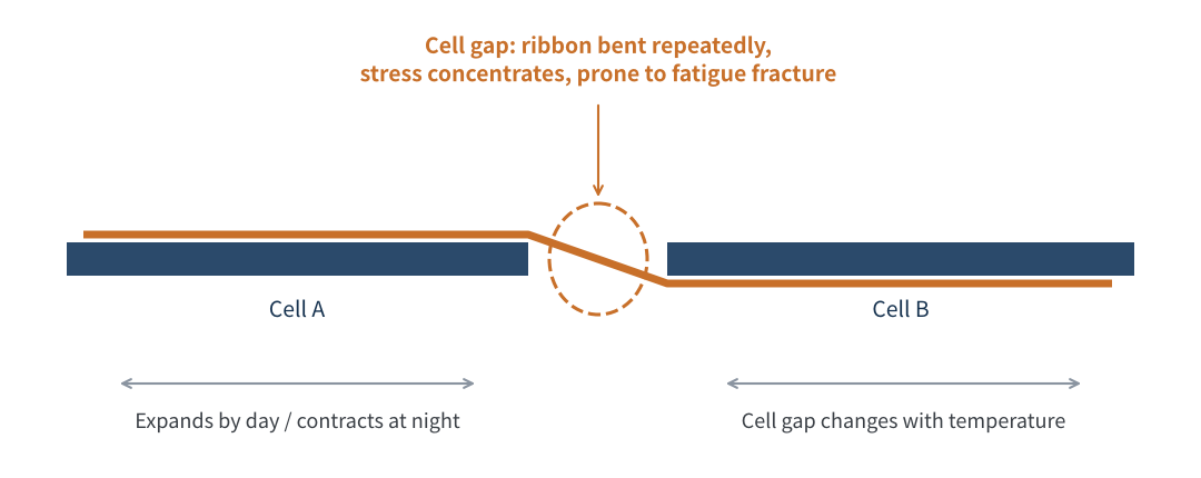
Figure 4 Repeated bending of ribbon in the gap between cells (schematic)
Between two cells, the ribbon has to "step down" from the front of one cell to the rear of the next. This short segment has no cell beneath it for support and is where deformation along the whole ribbon is most concentrated:
- Thermal cycling: cells expand and contract with temperature, the cell gap changes repeatedly, and the interconnect ribbon is bent back and forth like a piece of wire.
- Mechanical load: wind and snow loads bend the module, putting the interconnect ribbon under tension and bending at the same time.
- Finer means more sensitive: fine round wire has a small cross-section, so the same deformation produces higher stress and shorter fatigue life. The smaller the cell gap, the tighter the bend radius and the worse the problem.
The consequences of interconnect ribbon breakage depend on how many ribbons break. In a multi-busbar module, if one or two break, current can still flow through the others, showing up as a local resistance rise and slight heating. If many break, or a whole string opens, current is forced through the bypass diode; for a common module with three bypass diode sections, the worst case loses about one third of its power outright (in half-cell modules the upper and lower halves are in parallel, so the actual loss depends on where the break is). The most dangerous case is "almost broken": poor contact at the break can cause local high temperature or even arcing, one source of burn marks and fire risk.
This also explains the purpose of the segmented ribbon and flattened-section designs discussed in the second article: an important aim is to reduce stress concentration in the cell gap and improve fatigue resistance.
The interconnect segment is the most vulnerable part of the ribbon. One or two broken ribbons is a resistance problem, a broken string is a power problem, and "almost broken" is a safety problem.
05Corrosion: slow attack in damp heat
Ribbon-related corrosion mainly occurs in damp, hot environments. The most common "culprit" is acetic acid from hydrolysis of EVA encapsulant: moisture enters the module through the backsheet or edges, and under damp heat the vinyl acetate in EVA breaks down to release acetic acid, which attacks solder, joint interfaces and the cell's silver fingers.
- Joint corrosion: tin and lead in the solder corrode, the bond between joint and metallisation weakens, and contact resistance rises.
- Finger corrosion: the contact interface between silver fingers and silicon is attacked and finger contact resistance rises. EL often shows gradual darkening from the cell edge or along the ribbon.
- Ribbon surface discolouration: the ribbon coating oxidises and blackens and the surrounding encapsulant yellows. The PCT and damp heat tests discussed in the fifth article judge exactly whether there is yellowing or blackening within 10 mm on either side of the ribbon.
The degree of corrosion depends on encapsulant type, backsheet water vapour transmission and flux residue. POE-type encapsulants do not produce acetic acid and are a common choice for glass-glass modules and humid regions; excess flux residue worsens corrosion, which is one reason stringing processes control flux quantity. In coastal and high-salt-mist areas, salt mist corrosion of ribbon and busbars also needs attention.
06Hot spots and burn marks: the "last mile" of failure
The cold joints, fatigue cracks, ribbon breakage and corrosion described above all lead to the same outcome: local resistance rises and local heating follows.
By Joule's law, heating power is proportional to the square of current times resistance. Wherever resistance rises at a joint or along a ribbon, that spot keeps heating and forms a hot spot. In infrared thermography, such hot spots often run along the ribbon or concentrate at joints and busbar connections. Long-term overheating leads to:
- Encapsulant yellowing and browning: strip-shaped discolouration along the ribbon reduces light transmission and lowers power further.
- Burn marks and backsheet damage: burn marks appear on cells and joints, and in severe cases the backsheet is scorched or even burned through; the burn marks counted in the IEA report are mostly of this kind.
- Safety risk: busbar joints and lead-out connections carry the highest current, so poor contact there produces the most heat and makes them the locations with the highest arc and fire risk.
So although the busbar area has seen little technical change, it is a key area to inspect in failure analysis. The higher the current, the lower the tolerance for poor soldering. The 2025 IEA PVPS report also specifically notes that badly soldered electrical contacts in junction boxes can leave bypass diodes effectively unconnected, leading to power loss in whole strings or even fire, and recommends checking bypass diode function on 100% of modules in production.
07Failure analysis: from symptom to root cause
For ribbon-related failures, we suggest a four-step approach, "symptom, location, dissection, root cause", with different analysis tools at each step:
| Step | Common tools | What it answers |
|---|---|---|
| Symptom | Visual inspection, IV curve | How much power was lost? Is FF or current down? Are there steps in the curve? |
| Location | EL, infrared thermography | Which cell, which ribbon, which joint? |
| Dissection | Peel test, metallographic cross-section, SEM/EDS | Is the joint cracked? How thick is the IMC? Are there corrosion products? |
| Root cause | Comparison with incoming material, process and test data | Is it the ribbon, the soldering process, the encapsulant or the operating environment? |
Table 1 Four-step analysis of ribbon-related failures
The IV curve is a good "first screen": rising series resistance shows up as a lower FF and a "softer" curve around the maximum power point; when ribbon breakage makes a bypass diode conduct, the IV curve shows a clear step.
Once the failure mode is identified, it needs to be "translated" back into the ribbon properties covered in earlier articles to really solve the problem:
| Failure mode | Possible ribbon-related root cause | Prevention |
|---|---|---|
| Cold joints | Thin or oxidised coating, storage beyond shelf life | Coating thickness and storage management (articles 3, 5) |
| Soldering cracks, warpage | High yield strength, excessive soldering temperature | Yield strength window, low-temperature soldering (articles 3, 6) |
| Joint fatigue cracking | Solder system, poor initial joint quality | Coating alloy choice, peel force control (articles 3, 6) |
| Interconnect ribbon breakage | Fine diameter, small cell gap, stress concentration | Segmented/flattened design, layout optimisation (article 2) |
| Corrosion, yellowing | Flux residue, encapsulant mismatch | Compatibility testing, encapsulant selection (article 5) |
| Hot spots, burn marks | End result of all the above | Focused control of soldering quality in the busbar area |
Table 2 Failure modes, ribbon-related root causes and prevention
Most ribbon-related failures do not "happen suddenly"; they are the long-term combined result of manufacturing defects, material properties and field stress. Only by understanding failures can we work back to fix them in materials, processes and design.
08Final thoughts
The greatest value of failure analysis is not in "classifying" a failure but in feeding conclusions back upstream: ribbon selection, process windows, incoming material specifications and module layout. Every failed sample is a "health report" on materials and processes.
This article looked at "individual failures". In the next one we widen the view to the whole module and look at ribbon's role in module reliability: how ribbon is stressed in TC, DH and mechanical load tests, how ribbon is matched with thinner cells, encapsulants and cell metallisation, and how ribbon selection can improve module reliability. What tricky ribbon-related failures have you come across in your own analysis? We would be glad to hear from you.
References
- IEA PVPS Task 13: Review of Failures of Photovoltaic Modules (IEA-PVPS T13-01:2014), https://iea-pvps.org/wp-content/uploads/2020/01/IEA-PVPS_T13-01_2014_Review_of_Failures_of_Photovoltaic_Modules_Final.pdf
- Gopalakrishna H. et al., Activation Energy for End-of-Life Solder Bond Degradation: Thermal Cycling of Field-Aged PV Modules, IEEE Journal of Photovoltaics 10(6), 1762–1771 (2020), https://www.osti.gov/pages/biblio/1770900
- IEA PVPS Task 13: Assessment of Photovoltaic Module Failures in the Field (2017), https://iea-pvps.org/key-topics/report-assessment-of-photovoltaic-module-failures-in-the-field-2017/
- Crack initiation and growth in PV module interconnection, Liverpool John Moores University, https://researchonline.ljmu.ac.uk/id/eprint/15724/
- IEA PVPS Task 13: Degradation and Failure Modes in New Photovoltaic Cell and Module Technologies (IEA-PVPS T13-30:2025), 2025-02, https://iea-pvps.org/wp-content/uploads/2025/02/IEA-PVPS-T13-30-2025-EX-SUMM-Degradation-and-Failure.pdf
A PV R&D and technology team with 10+ years of experience | In-depth technical knowledge sharing
Materials · Reliability · Failure Analysis · Standards & Certification · Products · Processes
Exploring AI + PV; collaboration welcome
Disclaimer:
1. Original content reflects the authors' personal views only, is for reference only and does not constitute investment advice.
2. Reposted and cited content is credited to its source, out of respect for original work.
3. Some content was produced with AI assistance (chart generation, data retrieval, concept explanations, etc.); the core framework and key content were written by our technical team and reviewed by people.
4. If anything is inaccurate or infringes your rights, please leave a message or contact us and we will deal with it.