
Ribbon: The Most Overlooked "Blood Vessel" in a PV Module
In brief
Ribbon is the only material in a module that plays three roles at once, electrical, mechanical and optical: it must carry current out with minimal loss, bond firmly without cracking the cell, and block as little light as possible. Starting from the current path, we use a set of estimates to unpack the balance between these three roles, as the first article in our PV ribbon series.
When people think of a module, they think first of cells, glass, encapsulant and frames. The thin copper ribbon is often dismissed as an "auxiliary material". Yet every ampere a module generates has to travel along the ribbon, and how well it is soldered, how much light it blocks and how much stress it carries are written directly into the module's power and lifetime. In this article we start with the most basic question: what does ribbon actually do in a module?
01What ribbon is: the module's "blood vessels"
PV ribbon is essentially a copper strip (or wire) coated with a tin alloy. The copper conducts; the coating solders: during stringing the coating melts and joins the ribbon to the cell's fingers and busbars.
By position in the module, ribbon falls into two types:
- Interconnect ribbon: also called tinned ribbon or stringing ribbon. Thin and numerous, it connects the front of one cell to the back of the next, linking cells into a "string".
- Busbar ribbon: wide and flat, located at the ends of the strings, it collects current from each string and finally leads it to the junction box.
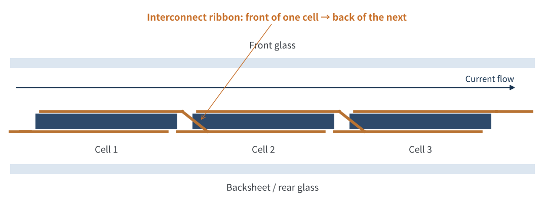
Figure 1 How interconnect ribbon connects cells in series (side view, schematic)
If the cells are the "organs", interconnect ribbons are the capillaries, busbar ribbons the aorta, and the junction box the heart's outlet. The complete current path is: cell fingers collect the current → interconnect ribbons connect cells in series → busbar ribbons collect the strings → the junction box leads current out to external cables.
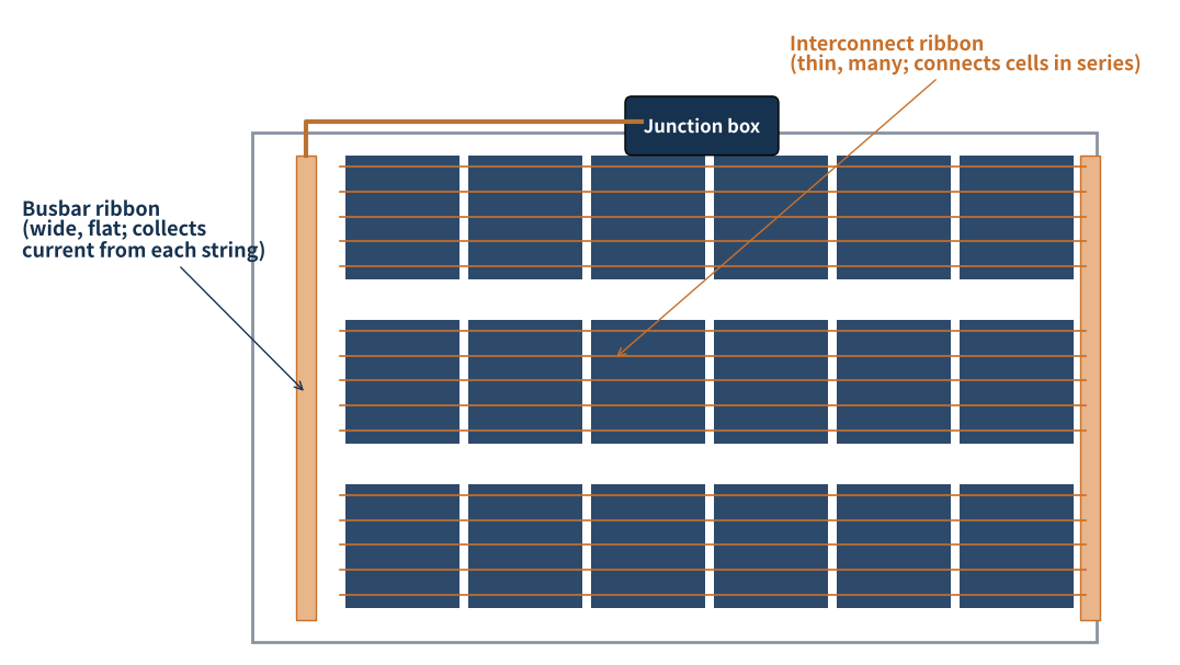
Figure 2 Position of interconnect and busbar ribbons in a module (top view, schematic, not to scale)
Simple as it looks, ribbon plays three roles in a module at once: conduction, connection and optics. Let us take them one by one.
02Role one: conduction, carrying current out with minimal loss
The most direct job of ribbon is to conduct. Wherever current flows there is resistive loss, and the loss is proportional to the square of the current (P = I²R). This is one reason half-cut cells increase power: halving the cell halves the current in each ribbon, cutting the resistive loss in the ribbon to about a quarter.
Let us estimate with a simplified data set (see the calculation notes at the end): for 182 half-cut cells with 16 round-wire ribbons of 0.26 mm diameter, the resistive loss in the ribbons alone is about 1.3% of cell power.
1.3% may not sound like much, but on a 600 W-class module it is several watts. So ribbon conductivity is a hard requirement:
- Substrate purity: high-purity oxygen-free copper is generally used; fewer impurities mean lower resistivity.
- Cross-sectional area: for the same material, a larger cross-section means lower resistance, but also more shading and stress, the conflict we will come to below.
- Coating: tin alloy coatings conduct far worse than copper; too thick a coating wastes "effective conductive cross-section".
Resistive loss in ribbon is proportional to the square of the current; there are only two ways to cut it: reduce the current in each ribbon (half-cut cells, multi-busbar) or increase the conductive cross-section.
03Role two: connection, bonding firmly without damaging the cell
Ribbon must form reliable solder joints with the cell. During soldering, the coating melts and forms an alloy interface with the cell's (silver) electrodes, which sets on cooling. Joint strength is commonly measured in the industry by peel force.
But "bonding firmly" is only half the story. The other half is not "pulling the cell apart". The problem is thermal expansion:
- Very different expansion coefficients: copper's coefficient of linear expansion is about 17×10⁻⁶/K, silicon's only about 2.6×10⁻⁶/K, a difference of more than sixfold.
- Stress from cooling after soldering: soldering takes place at two to three hundred degrees Celsius; on cooling to room temperature, copper shrinks more than silicon, setting the joint and cell "against each other", which shows up as warpage, micro-cracks or even breakage.
- Repeated loading outdoors: day-night temperature swings outdoors reapply the same stress again and again, leading over time to solder joint fatigue, one of the failure modes assessed by thermal cycling (TC) tests.
So ribbon is usually annealed to make it "soft", keeping its yield strength in a suitable range: too hard, and stress is passed to the cell; too soft, and it stretches and deforms in production. The thinner the cell, the narrower this window.
Different cell technologies also have different soldering temperature requirements. Heterojunction (HJT) cells, for example, have amorphous silicon layers and transparent conductive films that cannot tolerate high temperatures, so they need ribbon with low-temperature coatings such as tin-bismuth, or non-soldered interconnection such as conductive adhesive or film.
Ribbon's "connection" role is essentially a balance between solder reliability and cell stress; the thinner the cell and the lower the process temperature, the more demanding the ribbon material requirements.
04Role three: optics, every ribbon "blocks light"
Ribbon is opaque copper lying on the front of the cell, so it inevitably blocks some light. This is the most easily overlooked aspect of ribbon, yet it has a big impact on power.
The industry has two responses: make ribbon thinner, and change its cross-sectional shape. The flat surface of a flat ribbon reflects light largely out of the module; the sloped surfaces of round-wire and triangular or other shaped ribbons reflect some light at steep angles onto the glass surface, from where total internal reflection sends it back to the cell, "recovering" part of the blocked light.
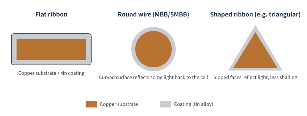
Figure 3 Common ribbon cross-sections (schematic)
Here is the catch: thinner ribbon blocks less light but has higher resistance. Let us calculate both together (still the simplified model of 16 round wires on 182 half-cut cells):
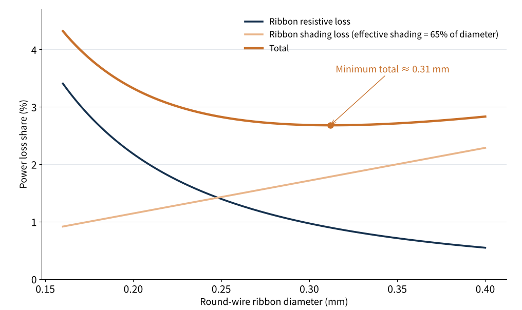
Figure 4 Trade-off between ribbon diameter, resistive loss and shading loss (simplified estimate)
As the diameter falls from 0.30 mm to 0.18 mm, shading loss decreases but resistive loss rises faster; the combined minimum is at about 0.31 mm. With the number of wires fixed, thinner ribbon is not always better.
So why does the industry keep making ribbon thinner and more numerous? Because the model above only counts the ribbon itself. With more busbars, current travels a shorter distance along the cell's fingers, reducing both finger resistive loss and silver paste consumption. "Thinner and more" is the system optimum, not the optimum for the ribbon alone, and that is the underlying logic of the progression from 5BB to MBB, SMBB and on to 0BB.
| Role | Key parameters | Consequences of imbalance |
|---|---|---|
| Conduction | Copper purity, cross-section, resistivity | Power loss, heating |
| Connection | Coating composition and thickness, yield strength, peel force | Cold joints, micro-cracks, solder joint fatigue |
| Optics | Diameter, cross-sectional shape, surface reflection | Shading loss, lower power |
Table 1 Key parameters and consequences of imbalance for ribbon's three roles
05A small material that carries real weight
Ribbon is not a conspicuous share of module cost, but it carries real weight in non-silicon costs. According to ChYXX (Zhiyan Consulting), PV ribbon accounts for about 12% of module non-silicon cost, and China's ribbon market was worth about RMB 29.8 billion in 2024, up about 39% year on year. Note that market size estimates vary widely between organisations: Qianzhan Industry Research Institute, counting "high-conductivity tinned ribbon" separately, puts that segment at about RMB 7.87 billion in 2025, with the penetration of high-conductivity products rising from 17.3% in 2023 to 31.7% in 2025.
In terms of industry structure, ribbon makers are mostly private companies and the market is not highly concentrated. According to Guanyan Report data, the top five held about 43% combined in 2021, with Yubang New Materials and Tongxiang Technology first and second, followed by Taiyang Technology, Tailisong, Wetown and others. In August this year, Yubang New Materials announced that its controlling shareholder and actual controllers are planning a change of control, so the landscape is also shifting. We will cover this in a later article in the series.
Ribbon pricing is essentially "copper price plus processing fee", so copper price swings pass straight through to module cost. On 8 September this year, LME copper hit a record USD 14,617 per tonne, up about 17% year to date; and ribbon design is tied to the cell's silver paste consumption. With both copper and silver prices high, the choice of ribbon solution is no longer just about the ribbon.
Another variable comes from standards: China's mandatory module efficiency standard GB 47834-2026 takes effect on 1 January 2027, with efficiency thresholds drawn in steps of 0.1 percentage points. By our estimate, ribbon resistance and shading together account for about 2.8% of cell power (at 0.26 mm diameter), one of the few areas at module level where a few tenths of a percentage point of efficiency can still be "squeezed out".
Ribbon is the only material in a module responsible for conduction, connection and shading at once, and each upgrade rebalances these three.
06Final thoughts
Ribbon is like the module's blood vessels: invisible most of the time, but when something goes wrong, it directly affects the "health" of the whole module. Understanding its three roles means understanding the starting point of every later development in ribbon technology: why round wire, why low temperature, why 0BB.
In the next article, we will look at ribbon structure and classification: from flat ribbon to round wire and shaped ribbon, and the different ribbon requirements of different cell technologies. What problems have you met in ribbon selection or the stringing process? We would be glad to hear from you.
References
- ChYXX (Zhiyan Consulting): Analysis of China's PV ribbon industry chain, status, competitive landscape and trends, 2025
- Guanyan Report: Analysis of the current state of China's PV ribbon industry, 2022-11
- Qianzhan Industry Research Institute: Market size and competitive landscape of high-conductivity tinned ribbon, 2026-05
- Gelonghui: LME copper prices hit successive record highs, 2026-09-08
- Yubang New Materials suspension announcement on the planned change of control by its controlling shareholder and actual controllers, 2026-08 (reported by 10jqka)
- GB 47834-2026, Minimum allowable values of energy efficiency and energy efficiency grades for crystalline silicon PV modules and inverters
- Thermal expansion coefficients of copper and silicon and the resistivity of copper are general physical data, using common reference values.
A PV R&D and technology team with 10+ years of experience | In-depth technical knowledge sharing
Materials · Reliability · Failure Analysis · Standards & Certification · Products · Processes
Exploring AI + PV; collaboration welcome
Disclaimer:
1. Original content reflects the authors' personal views only, is for reference only and does not constitute investment advice.
2. Reposted and cited content is credited to its source, out of respect for original work.
3. Some content was produced with AI assistance (chart generation, data retrieval, concept explanations, etc.); the core framework and key content were written by our technical team and reviewed by people.
4. If anything is inaccurate or infringes your rights, please leave a message or contact us and we will deal with it.