
From Flat Ribbon to Round Wire: PV Ribbon Structure and Classification Explained
In brief
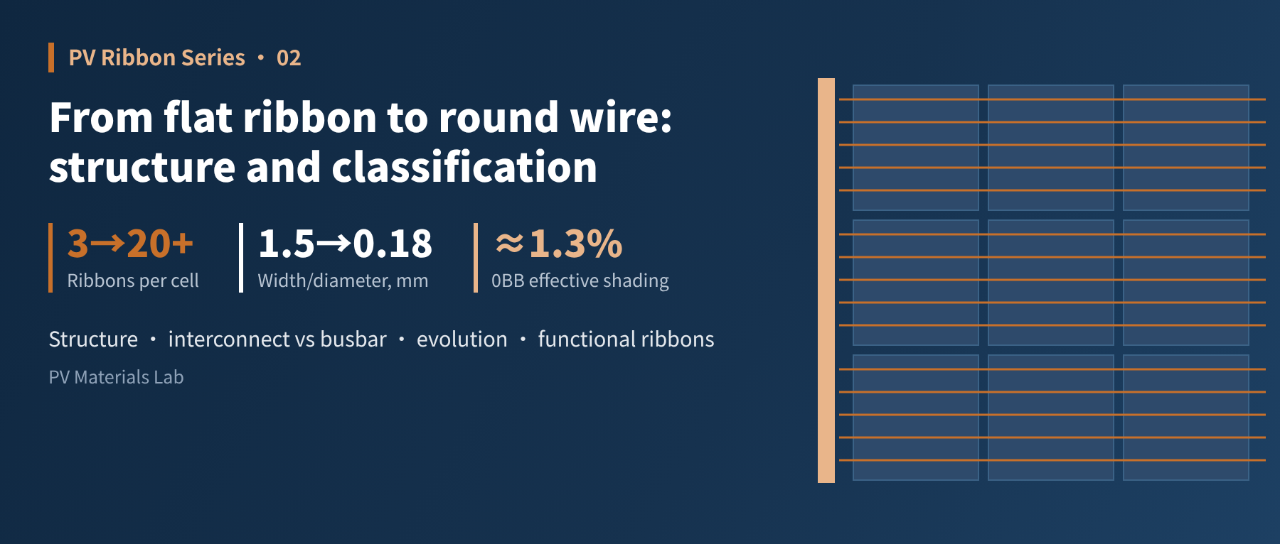
A ribbon consists of a copper substrate and a tin alloy coating, and by use it divides into interconnect ribbon and busbar ribbon. Over the past decade, interconnect ribbon has evolved from 1.5 mm-wide flat strips to round wires of around 0.2 mm and a variety of shaped ribbons, while different cell technologies have spawned niches such as low-temperature and BC-specific ribbons. We take apart ribbon structure, map the main categories, and use a set of estimates to show that while the number of ribbons has multiplied, shaded area has barely increased.
In the previous article we covered ribbon's three roles in a module: conduction, connection and optics. These three pull in different directions: good conduction argues for thicker ribbon, less shading for thinner, and avoiding cell damage for softer. Every change in ribbon form over the past decade has been a rebalancing of these three. In this article we look at what ribbon looks like, how it is classified, and why it has ended up the way it is today.
01Anatomy of a ribbon: copper substrate + coating
However its shape changes, the basic structure of ribbon is simple: a copper substrate in the middle, wrapped in a tin alloy coating. Each part has its own job:
- Copper substrate: handles conduction and mechanical support. High-purity oxygen-free copper is usually used; the higher the purity, the lower the resistivity. Annealing then controls its hardness (yield strength) so it does not crack the cell after soldering.
- Coating: handles soldering. During stringing the coating melts and forms solder joints with the cell's fingers and busbars; it also protects the copper from oxidation. Coating thickness is generally on the order of ten to several tens of micrometres.
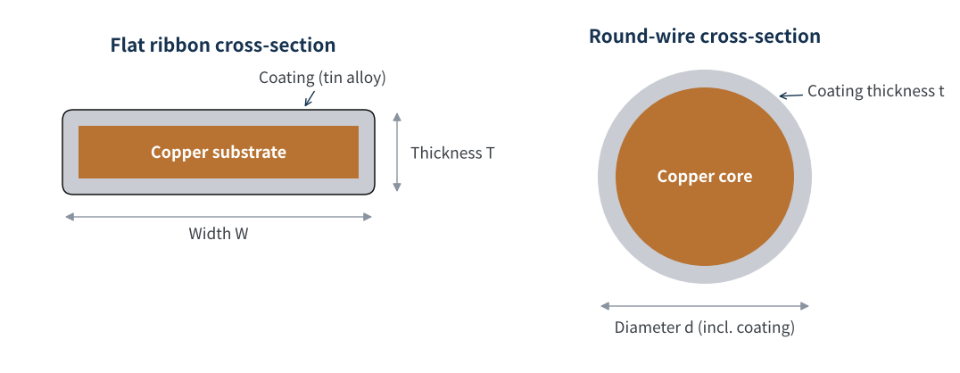
Figure 1 Cross-sections of flat ribbon and round-wire ribbon (schematic)
Why not solder bare copper directly, or just use pure tin strip? Simply because bare copper cannot form reliable solder joints with the electrodes directly and oxidises easily, while pure tin conducts only about one-seventh as well as copper and lacks strength. "Copper as the skeleton, tin as the skin" is the compromise between conduction, soldering and cost.
The coating may be thin, but it requires care. Too thin, and there is not enough solder, risking cold joints and low peel force; too thick or uneven, and excess solder may overflow into solder balls while taking up cross-section that hardly conducts. For round wire, whether the coating is concentric and even all round directly affects the amount of solder at the contact surface during soldering.
To describe a ribbon, the industry usually looks at these parameters:
| Parameter | Meaning | What it affects |
|---|---|---|
| Width × thickness / diameter | Cross-sectional dimensions | Resistance, shading, stress |
| Coating composition | Tin-lead, tin-lead-silver, tin-bismuth, etc. | Soldering temperature, solderability, environmental compliance |
| Coating thickness | Thickness and uniformity of coating per side | Peel force, risk of cold joints |
| Resistivity | Conductivity of the material | Power loss |
| Yield strength / elongation | Hardness and ductility of the copper | Micro-cracks, breakage, stretching |
Table 1 Main ribbon parameters
These parameters will be covered in detail in the third article on "materials" and the fifth on "test methods". For now, note that every ribbon parameter maps to one of the roles of conduction, connection or optics.
02Two main types: interconnect ribbon vs busbar ribbon
By use in the module, ribbon first divides into two main types. This is the most basic classification and the one used throughout the industry:
| Interconnect ribbon | Busbar ribbon | |
|---|---|---|
| Common names | Tinned ribbon, stringing ribbon | Busbar, bus ribbon |
| Location | Front and back of cells | Ends of strings, lead-out wires |
| Function | Connects cells in series into strings | Collects current from strings and leads it to the junction box |
| Form | Thin, flat strip or round wire, a dozen to twenty-plus per cell | Wide and flat, typically a few millimetres wide |
| Pace of change | Fast, iterating frequently with cell technology | Slow, mainly cost reduction and thinning |
Table 2 Interconnect ribbon vs busbar ribbon
Yubang New Materials' 2025 annual report defines the two plainly: interconnect ribbon is "soldered directly onto the front and rear electrode positions of the cell", connecting adjacent cells in series and conducting power out; busbar ribbon is tinned ribbon that "leads current from the series-parallel connected cell strings to the junction box".
Interconnect ribbon is the fastest-changing and most technically demanding part, and the focus of this series. Busbar ribbon has changed little, but it carries the largest current, and its solder joints and lead-outs at the ends of the module are hot spots for hotspot and overheating problems.
The main changes in busbar ribbon in recent years have been twofold: first, thinning, because thicker busbars create more pronounced bumps between glass and backsheet after lamination, with greater local stress; second, adapting to module layouts, such as centre busbars for half-cut layouts, folded designs that reduce edge margins, and pre-punched or pre-formed lead-outs, all aimed at saving space and copper without increasing resistance.
Interconnect ribbon "strings"; busbar ribbon "collects". The former iterates quickly with cell technology; the latter evolves slowly with module layout and cost reduction.
03Evolution of form: from flat ribbon to round wire
The form of interconnect ribbon has broadly followed the number of busbars on the cell. It can be divided into roughly four stages:
- 3BB–5BB, the flat-ribbon era: cells were printed with 3–5 fairly wide silver busbars, and ribbon was flat with a rectangular cross-section, its width falling gradually from about 1.5 mm to below 1 mm.
- MBB, round wire arrives: busbars increased to 9–12, and ribbon became round wire 0.3–0.4 mm in diameter. With more wires, current is shared among more ribbons, and current travels a shorter path along the fingers.
- SMBB, thinner and more: busbars increased further to 16 or more, with round-wire diameter down to 0.2–0.3 mm. This has been the mainstream solution for TOPCon modules in recent years.
- 0BB, no busbars: busbars are no longer printed on the cell; ribbon contacts the fingers directly and is held by film or dispensed adhesive; wire diameter falls below 0.2 mm, with 20 or more wires.
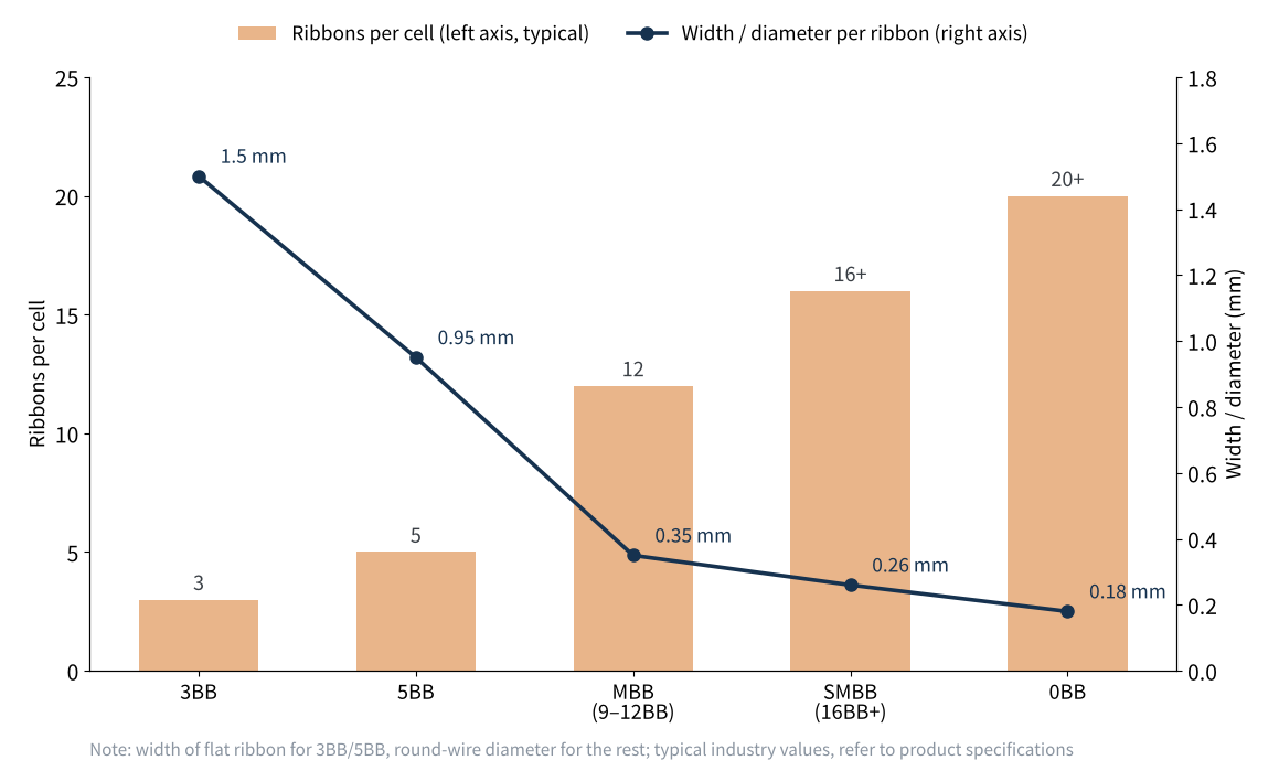
Figure 2 Evolution of interconnect ribbon count and size (typical industry values, schematic)
Why change like this? Two core drivers: saving silver and reducing shading.
First, silver. Busbars are printed silver paste, so the higher the silver price, the more "expensive" the busbars. More, finer busbars use less silver paste; 0BB removes busbars entirely, cutting silver consumption further. This matters especially with silver prices high: measured by London spot silver, the price rose from about USD 29/oz at the start of 2025 to about USD 71.6/oz at year end, up about 147% for the year, and briefly broke above USD 80/oz. According to industry reports, progressive silver-reduction technologies including 0BB and fine-line printing are now fully deployed by leading manufacturers such as JinkoSolar, JA Solar and Trina Solar, cutting TOPCon silver consumption from about 12 mg/W in 2023 to about 9 mg/W, a saving of about 25%.
As the form changed, manufacturing had to change too. Round wire makes "line contact" with the cell, so each solder joint is very small, demanding greater consistency in soldering temperature, pressure and ribbon coating; with more wires, stringers must pull and position a dozen to twenty-plus fine wires at once, and any one drifting can cause cold joints or cover fingers. With 0BB, ribbon is no longer positioned by busbar pads; instead it is first "pressed" onto the cell with film or dispensed adhesive, and the connection between ribbon and fingers is completed during lamination. The finer the ribbon, the stricter the demands for "straight, round and even": diameter tolerance, straightness and coating uniformity are all magnified.
Now shading. Many people assume that going from 5 to 20 ribbons must multiply shading several times. In fact it does not. Here is an estimate on a common basis using 182 mm cells (see the calculation notes at the end):
| Stage | Count × size | Geometric shaded width | Effective shading share (est.) |
|---|---|---|---|
| 3BB | 3 × 1.5 mm flat | 4.5 mm | About 2.5% |
| 5BB | 5 × 0.95 mm flat | About 4.8 mm | About 2.6% |
| MBB | 12 × 0.35 mm round | About 4.2 mm | About 1.5% |
| SMBB | 16 × 0.26 mm round | About 4.2 mm | About 1.5% |
| 0BB | 20 × 0.18 mm round | About 3.6 mm | About 1.3% |
Table 3 Estimated ribbon shading by stage (all on 182 mm cells)
As you can see, the number of ribbons has multiplied several times, yet geometric shaded width is essentially unchanged and effective shading has actually fallen by about half. The secret lies in the cross-sectional shape; that is the optical significance of moving from flat ribbon to round wire.
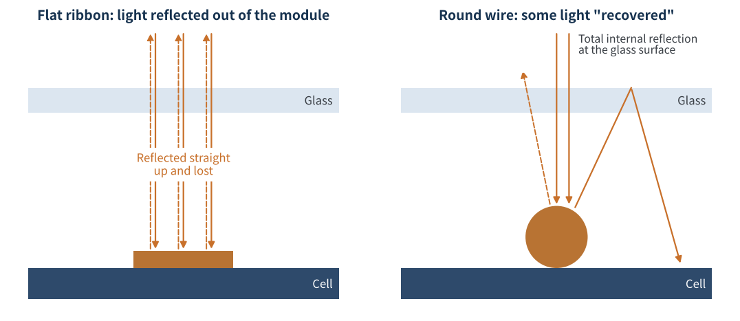
Figure 3 Light paths for flat ribbon and round wire (schematic)
A flat ribbon's surface is flat, so light hitting it is reflected almost straight back out of the module and wasted. A round wire's surface is curved: light hitting its "shoulders" is reflected out at a steep angle, undergoes total internal reflection at the glass surface and returns to the cell. In other words, a good part of the light blocked by round wire is "recovered".
Moving from flat ribbon to round wire, ribbon has gained "more wires" while keeping "less shading", and has helped cells save large amounts of busbar silver paste. It is a simultaneous optimisation of electrical, optical and cost performance.
04Shaped ribbon: working between "shading" and "contact"
Round wire solved the shading problem but brought new trouble: it makes "line contact" with the cell, so the soldered area is small and contact is poor; pressed onto the back of the cell, it also increases local stress during lamination. Hence a variety of shaped ribbons:
- Triangular ribbon: a triangular or near-triangular cross-section, point up and base down. The sloped faces reflect light back to the cell, while the flat base contacts the electrodes, balancing optics and soldering.
- Segmented ribbon: one ribbon divided into segments of different shapes: a round-wire segment on the front for less shading, a flattened segment on the back to reduce thickness and stress, and a transition segment spanning the gap between cells.
- Oval ribbon: a cross-section between flat and round, keeping some of the reflective effect of the curved surface while widening the contact with the electrodes.
- Light-reflecting ribbon: fine V-grooves or other microstructures pressed into the surface of flat ribbon turn vertical reflection into oblique reflection, so flat ribbon too can "recover" some light.
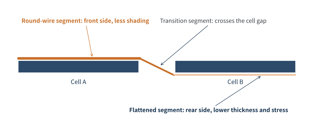
Figure 4 Segmented ribbon: round-wire segment on the front + flattened segment on the back (schematic)
Segmented ribbon deserves a further word. The smaller the gap between cells, the more compact the module layout and the higher its efficiency, but the greater the bending stress as the ribbon "steps down" between cells. Segmented design lets the ribbon "do a different job in each place", making it an important enabling technology for compact layouts such as small-gap and overlapping (shingled-type) stringing.
What shaped ribbons have in common is more complex processing, higher precision requirements, and greater demands on stringers' threading and positioning capabilities. This is one of the main battlegrounds where ribbon makers differentiate themselves technically.
05By cell technology: different cells, different ribbons
Besides form, cell technology itself sets "questions" for ribbon. Different cells have different requirements for soldering temperature, electrode structure and light-receiving surfaces, and ribbon has diversified accordingly:
| Cell technology | Main requirements for ribbon | Typical solution |
|---|---|---|
| PERC | Conventional soldering temperature, mature technology | MBB/SMBB round wire with conventional coating |
| TOPCon | Bifacial; finer, denser fingers | SMBB round wire, shaped ribbon; 0BB being introduced |
| HJT | Amorphous silicon and transparent conductive films not heat-tolerant | Low-temperature coated ribbon (e.g. tin-bismuth), or 0BB film interconnection |
| BC | Both electrodes on the rear, no front shading | Rear-side dedicated ribbon that must prevent shorting between positive and negative |
Table 4 Ribbon requirements of different cell technologies
Two kinds of "functional" ribbon deserve particular mention:
- Low-temperature ribbon: conventional tin-lead alloy melts at about 183 °C, and soldering temperatures are usually higher still; tin-bismuth alloy has a eutectic melting point of about 139 °C, lowering soldering temperature significantly. It first served mainly HJT, and as cells get thinner, the need to reduce soldering thermal stress is spreading to other technologies.
- BC-specific ribbon: BC cells have no electrodes on the front, so all ribbon is on the back and no longer constrained by shading; in principle it can be wider and flatter to reduce resistance. But positive and negative electrodes are interdigitated, so ribbon must be precisely aligned and kept from shorting by insulation or structural design.
There are also categories defined by appearance or environmental requirements, such as black ribbon for all-black modules and lead-free ribbon to meet environmental rules. Their structure changes little; the main differences lie in the coating and surface treatment.
Ribbon classification follows three lines: by use, interconnect and busbar; by form, flat, round wire and shaped; by need, functional types such as low-temperature, BC, black and lead-free.
06How to choose: four questions
With classification covered, in practice, when a module maker introduces a new ribbon, we suggest asking four questions in order:
- What is the cell technology? First settle the coating system and soldering temperature. HJT and ultra-thin cells should look first at low-temperature solutions; for BC, look at the rear electrode layout and insulation scheme.
- What is the electrode design? The number of busbars determines the number and diameter of ribbons; 0BB also involves fixing methods such as film or dispensed adhesive, so ribbon and auxiliary materials must be validated together.
- What constraints does the layout impose? The smaller the cell gap and the tighter the overlap, the more shaped designs such as segmented or flattened ribbon are needed to relieve stress; in the busbar area, watch busbar thickness and folding.
- Who is the product for? All-black rooftop modules may need black ribbon; for export to markets with strict restrictions on hazardous substances, assess the soldering window and reliability of lead-free coatings in advance.
Once these four questions are answered, comparing suppliers on dimensional tolerance, yield strength, coating uniformity and price becomes meaningful. Settle the solution first, then compare parameters, and you will avoid many detours.
07Final thoughts
Looking back at the evolution of ribbon, a clear logic emerges: wherever cell technology goes, ribbon follows. More busbars, so ribbon becomes thinner and round; cells that fear heat, so ribbon lowers its melting point; electrodes moved to the back, so ribbon no longer fears shading. A ribbon maker's job is to stay "half a step ahead" of cell technology.
This article covered ribbon's "form". In the next one we go into its "substance", that is, ribbon materials: how to choose oxygen-free copper, the ins and outs of coating systems, and whether cost-saving materials such as copper-clad aluminium can be used. What problems have you met in selecting or introducing ribbon? We would be glad to hear from you.
References
- ChYXX (Zhiyan Consulting): Classification and development trends of China's PV ribbon industry
- Yubang New Materials 2025 annual report summary (definitions of interconnect and busbar ribbon), Shanghai Securities News, 2026-04-17
- PV Manufacturing: Multi-Busbars Solar Cells & Modules
- TMTPost (Gantanhao Technology): Overview of PV silver-reduction technology routes (silver price and silver consumption per watt), 2026-01-05
- Melting points of tin-lead and tin-bismuth alloys and resistivities of copper and tin are general physical data, using common reference values.
A PV R&D and technology team with 10+ years of experience | In-depth technical knowledge sharing
Materials · Reliability · Failure Analysis · Standards & Certification · Products · Processes
Exploring AI + PV; collaboration welcome
Disclaimer:
1. Original content reflects the authors' personal views only, is for reference only and does not constitute investment advice.
2. Reposted and cited content is credited to its source, out of respect for original work.
3. Some content was produced with AI assistance (chart generation, data retrieval, concept explanations, etc.); the core framework and key content were written by our technical team and reviewed by people.
4. If anything is inaccurate or infringes your rights, please leave a message or contact us and we will deal with it.