
Is 1.25 × Isc Enough? Calculating the Thermal-Runaway Boundary of Bypass Diodes in High-Gain Bifacial Applications
INFO
The bypass diode in a junction box spends most of its life idle. The moment a module is partially shaded, it has to carry the full string current. Certification tests check its junction temperature at 1.25 × Isc, and many engineers assume that 1.25 is a safety factor. Put a bifacial module over snow or a white-painted roof, add the irradiance boost at cloud edges, and that factor gets eaten away. In this article we do the math: how much current does the diode really carry in the field, how hot does it get, and where does it tip into thermal runaway?
01 How the Standard Tests It: Where 1.25 × Isc Comes From
The bypass diode thermal test MQT 18.1 in IEC 61215-2 is familiar: heat the module to (75 ± 5) °C, apply the STC short-circuit current for 1 h and determine the junction temperature, then raise the current to 1.25 × Isc for another hour; the diode must still work afterwards. The pass criterion is that the junction temperature stays below the manufacturer's maximum rating for continuous operation.
That 1.25 is essentially an operating assumption: it presumes field current never exceeds STC by more than 25 % — roughly 1250 W/m² of equivalent irradiance. For monofacial modules this holds in most places.
The standard was revised for bifacial modules. IEC 61215:2021 rates power at 135 W/m² rear irradiance (BNPI), while every test whose stress level is set by measured current uses a near-worst-case rear irradiance of 300 W/m² (BSI). The bypass-diode test current becomes 1.25 × Isc(1000 + φ·300).
Summary
The standard verifies cooling at an assumed maximum current. The real question is whether that assumption covers the place your module is actually going.
02 Field Reality: Three Currents Stacked Together
When a bypass diode conducts, its current roughly equals the operating current of the other modules in the string, which scales almost linearly with total irradiance. For a bifacial module:
Equivalent irradiance = front irradiance + φ × rear irradiance
where φ is the bifaciality. Three field factors push it up at the same time:
- High-albedo ground: fresh snow has an albedo of about 0.82, wet snow 0.55–0.75; a freshly coated white roof can reach around 0.7 (lower after ageing). The brighter the ground, the higher the rear irradiance.
- Higher bifaciality: TOPCon modules typically sit around 0.8, HJT higher. The same rear light yields more current.
- Cloud-edge enhancement: with cumulus near the sun, light scattered at cloud edges adds to the direct beam and ground irradiance briefly exceeds clear-sky values. Measurements in Finland peaked near 1450 W/m², about 1.7 × the local clear-sky maximum; 11 months of data in San Diego peaked at 1466 W/m²; southern Norway recorded a 1528 W/m² burst, and values above 1800 W/m² have been reported near the equator.
Taking a module with Isc(STC) = 18.4 A and φ = 0.80 as an example (Figure 1):
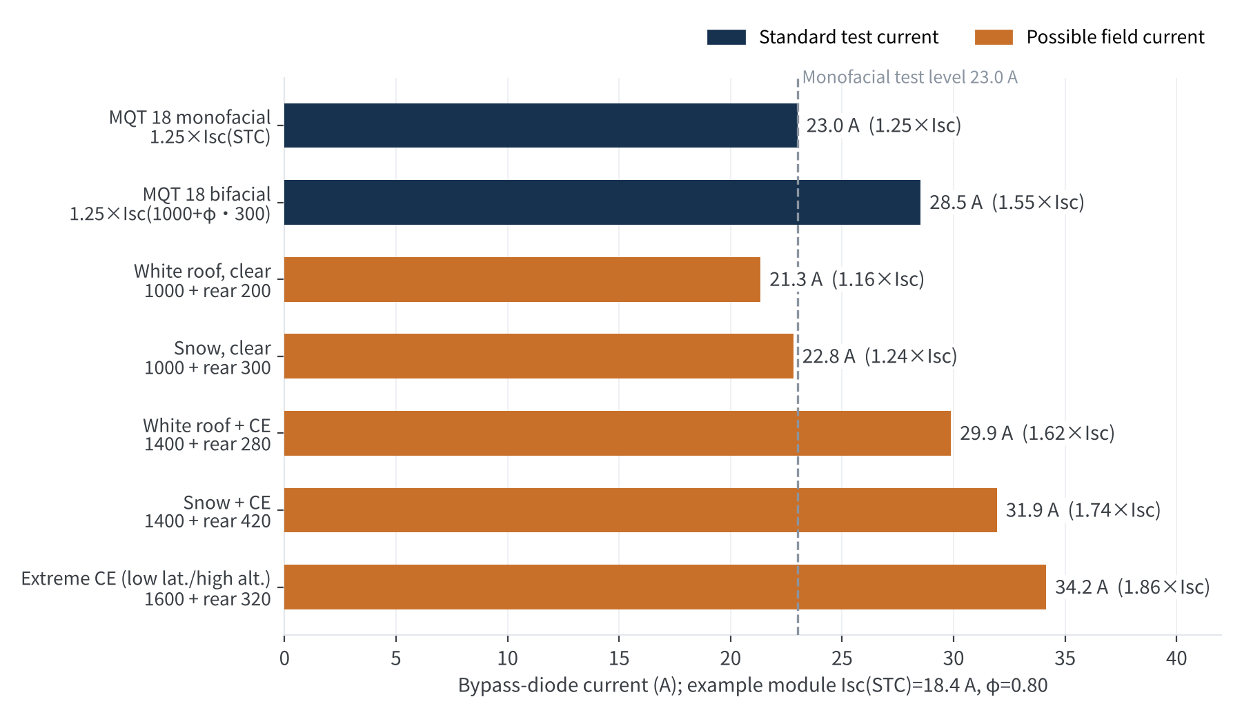
Figure 1 Bypass-diode current under different conditions
| Condition | Front / rear irradiance (W/m²) | Diode current | Relative to monofacial test |
|---|---|---|---|
| MQT 18, monofacial | 1.25 × STC | 23.0 A | 1.00 |
| MQT 18, bifacial | 1.25 × (1000 + φ·300) | 28.5 A | 1.24 |
| White roof + cloud enhancement | 1400 / 280 | 29.9 A | 1.30 |
| Snow + cloud enhancement | 1400 / 420 | 31.9 A | 1.39 |
| Extreme enhancement (low latitude / high altitude) | 1600 / 320 | 34.2 A | 1.48 |
The monofacial 1.25 factor is exceeded by 30–50 % in high-gain scenarios. Even against the 2021 bifacial test level, snow or white roofs combined with cloud enhancement are another 5–20 % higher.
Bottom line
For bifacial modules, 1.25 × Isc is no longer a ceiling. Real current can reach 1.6–1.9 × the STC short-circuit current.
03 Gate One: Forward Junction Temperature
More current means more heat: P = Vf × I. A Schottky diode at high temperature and high current has Vf of roughly 0.4–0.5 V, so a single diode dissipates about 14 W at 30 A — all of which the junction box has to get rid of.
A simple steady-state estimate:
Tj = Tref + Rth × Vf × I
Tref is the module rear-surface temperature at the junction box, Rth the equivalent thermal resistance from junction to that point. We take Rth = 8 K/W, which puts the monofacial test result just above 150 °C, in line with common designs. Results are in Figure 2.
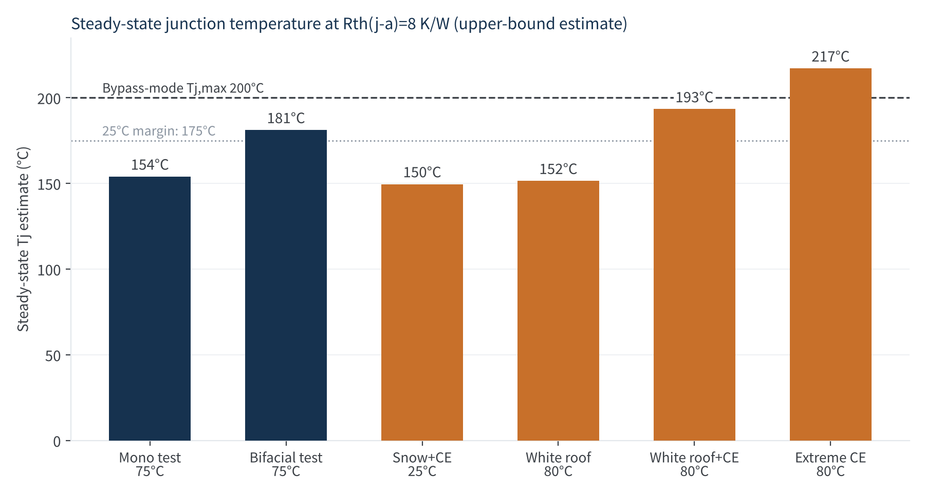
Figure 2 Estimated steady-state junction temperature at Rth = 8 K/W
There is an easily missed contrast:
- Snow gives the highest current but the coldest box. Winter rear temperatures are low; even at 32 A the steady-state Tj is only about 150 °C.
- White roofs give slightly less current but the hottest box. Poorly ventilated summer roofs easily see 80 °C near the junction box. With cloud enhancement the estimate reaches 193 °C — right against the 200 °C bypass-mode limit — and extreme enhancement breaks through it.
So the true worst case is often not the highest current but the condition where high current and high ambient temperature coincide.
Note that Figure 2 is an upper-bound steady-state estimate. A single enhancement event usually lasts seconds to minutes and the thermal mass of the diode and box clips the peak. That buffer is unreliable, though: on broken-cloud days enhancement events repeat and heat accumulates in the box.
Summary
Check gate one with maximum field current × maximum field temperature, not 1.25 × Isc at 75 °C.
04 Gate Two: Thermal Runaway — Danger Comes When the Diode Turns Off
If forward junction temperature is about surviving the heat, thermal runaway is about surviving the heat and then dying on the way back down.
Bypass diodes are mostly Schottky types: low Vf, less heat. The price is reverse leakage that rises exponentially with temperature, roughly doubling every 10 °C. One study measured a ~35 × increase in leakage when the junction box went from 25 °C to 70 °C.
The dangerous sequence is shown in Figure 3:
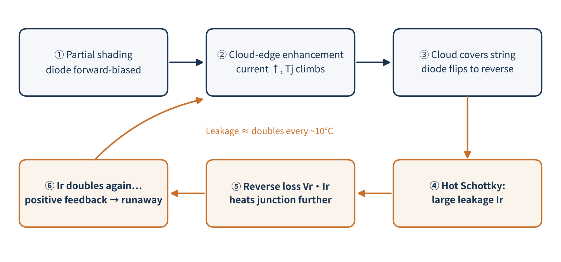
Figure 3 The positive-feedback loop of bypass-diode thermal runaway
Cloud-edge enhancement arrives just ahead of the cloud shadow. So the diode is heated to its peak by enhanced current, then the cloud covers the whole string, shading contrast vanishes, and the diode is suddenly reverse-biased by one substring voltage (about 12–13 V). It is still hot, leakage is high, and if the reverse loss Vr × Ir exceeds what the box can remove, junction temperature keeps climbing, leakage doubles again… until the diode breaks down, usually failing short.
A useful concept is the critical temperature Tcrit: the junction temperature at which reverse power equals forward power for a given current and reverse voltage. If the forward operating Tj is below Tcrit, the diode cools after switching; above it, it runs away. Tcrit depends only on the diode's Vf and leakage — not on the junction box thermal resistance.
We compare two illustrative diodes: A, low-Vf (higher leakage), and B, low-leakage (slightly higher Vf). Plotting forward operating Tj and Tcrit against current (Figure 4), the crossing point is the thermal-runaway boundary.
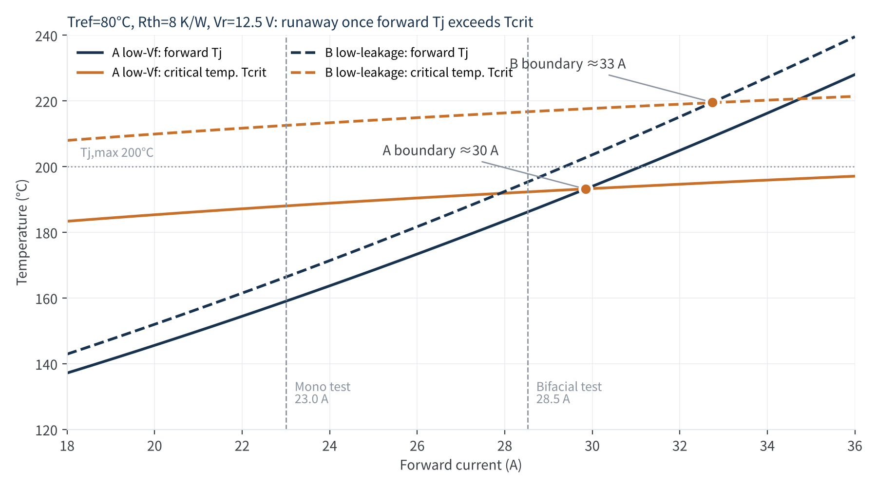
Figure 4 The crossing of forward Tj and Tcrit marks the runaway boundary
At Tref = 80 °C and Rth = 8 K/W:
- Diode A's boundary is about 30 A — right at the 29.9 A of the white-roof + cloud-enhancement case.
- Diode B's boundary is about 33 A, more margin; but with its higher Vf, its forward Tj already exceeds 200 °C at 30 A, so it fails gate one first.
This is the unavoidable Schottky trade-off: low Vf and low leakage rarely come together. Swapping diodes alone won't solve it; thermal resistance must come down too.
Now a dynamic case (Figure 5): diode A goes through ten cycles of "60 s enhanced / 30 s normal" on a broken-cloud day, then a cloud covers the string. At 8 K/W and Tref 80 °C it cools down smoothly after switching. At 10 K/W and an ambient 5 °C hotter, Tj crosses the critical point at the moment of switching and runs away.
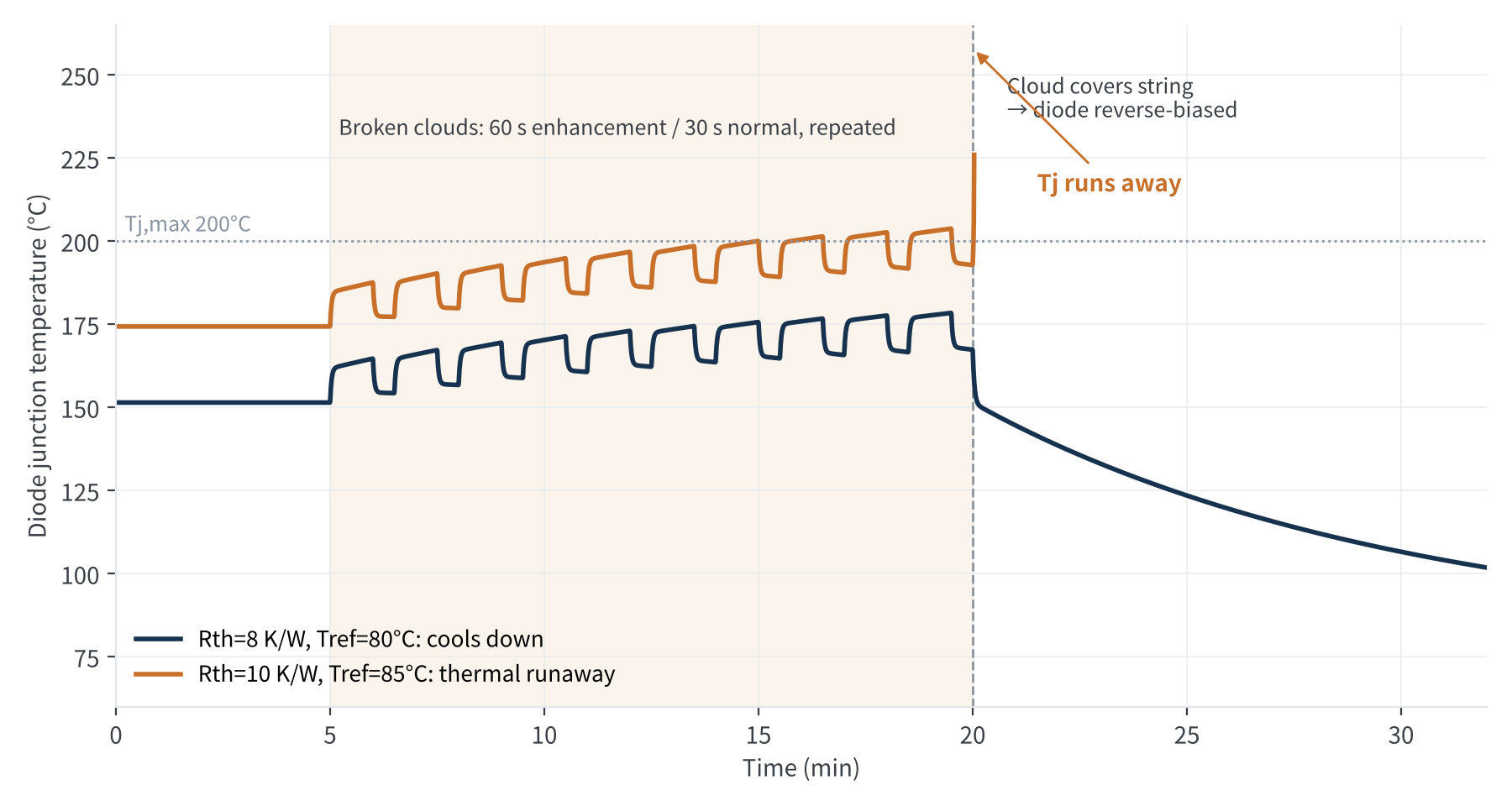
Figure 5 Switching to reverse bias after cloud enhancement: junction temperature under two cooling conditions (illustrative calculation)
Summary
The runaway boundary is steep: 2 K/W more thermal resistance and 5 °C more ambient can move a design from safe to runaway. IEC 62979 tests exactly this transition; P/N-junction diodes are exempt because their reverse-bias capability is high enough.
05 How to Derate for Real Operating Conditions
Putting it together, we suggest four steps (Figure 6):
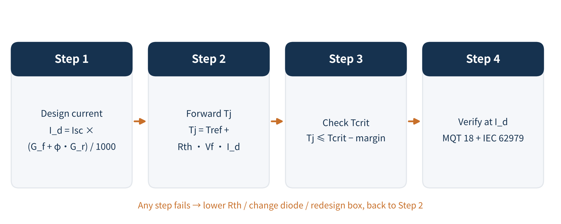
Figure 6 Four-step thermal derating method for bypass diodes
- Step 1 — Design current: take maximum front irradiance for the site (with cloud enhancement, typically 1400–1500 W/m², higher at low latitude and high altitude) and rear irradiance (set by albedo and mounting height), then I_d = Isc × (G_f + φ·G_r)/1000, with an extra factor for power binning and process spread if needed.
- Step 2 — Forward Tj: use the site's highest Tref (treat summer rooftops separately) and require Tj ≤ bypass-mode Tj,max − 25 °C. At 30 A and 80 °C, Rth must stay below about 6.7 K/W.
- Step 3 — Check Tcrit: derive Tcrit from the datasheet's high-temperature leakage curves and keep forward Tj at least 15–20 °C below it. Datasheet leakage is usually given at the rated 45 V — convert to the actual substring voltage.
- Step 4 — Verify at I_d: run MQT 18 and IEC 62979 at the design current, not the standard value, to see the real margin.
If any step fails, options include split junction boxes to avoid heat build-up per diode, larger copper / heat-spreader areas, better thermally conductive potting, relocating the box, or moving to active bypass (MOSFET ideal diodes) that cut forward drop to tens of millivolts.
Final Thoughts
1.25 × Isc is not a safety factor; it is an operating assumption. For monofacial modules over ordinary ground it largely holds. For bifacial modules over bright ground in cloudy, high-irradiance regions, it no longer does.
We recommend shifting bypass-diode selection from "passes certification" to "passes the site": first establish how much current the diode must carry, then check how much margin remains at both boundaries — forward junction temperature and the thermal-runaway critical temperature. A special note for distributed white-roof projects: the most dangerous day is often not the brightest one, but the bright, hot day with clouds on the move.
Next time we look at active bypass (ideal diode) solutions: can they remove both gates at once, and what new reliability questions do they bring?
Calculation Notes / Data Basis
- Example module: Isc(STC) = 18.4 A, bifaciality φ = 0.80; short-circuit current scaled linearly with equivalent irradiance, temperature coefficient ignored (about ±1 %).
- Rear irradiance taken as 20 % (white roof) to 30 % (snow) of front, an estimate based on albedo and typical mounting heights; real values vary strongly with height, row spacing and module position.
- High-temperature forward drop approximated as Vf = 0.28 + 0.0065 × I (V); diode B +0.04 V.
- Thermal resistance Rth(j-ref) = 8 K/W; dynamic calculation uses a two-node network (junction–box 2 K/W, 1 J/K; box–module 6 K/W, 100 J/K).
- Leakage: diode A 10 mA, diode B 2 mA at 125 °C and 12.5 V, extrapolated by doubling every 10 °C; reverse voltage = substring operating voltage 12.5 V.
- All parameters are illustrative and do not correspond to any specific product; results show trends and method. Use measured data for actual designs.
References
- IEC 61215-2:2021, Terrestrial photovoltaic (PV) modules – Design qualification and type approval – Part 2: Test procedures (MQT 18 bypass diode thermal test)
- IEC 61215-1:2021, Part 1: Test requirements (BNPI/BSI for bifacial modules); J. Wohlgemuth, NIST presentation "Qualification Standard (IEC 61215)"
- IEC 62979:2017, Photovoltaic modules – Bypass diode – Thermal runaway test
- K. Lappalainen, J. Kleissl, Analysis of the cloud enhancement phenomenon and its effects on photovoltaic generators based on cloud speed sensor measurements, 2020
- G. H. Yordanov et al., Overirradiance (Cloud Enhancement) Events at High Latitudes, IEEE Journal of Photovoltaics, 2013
- Tampere University, Experimental Observations about the Cloud Enhancement Phenomenon on PV Strings
- N. S. Shiradkar et al., Predicting Thermal Runaway in Bypass Diodes in Photovoltaic Modules, 2014
- Origin of Bypass Diode Fault in c-Si Photovoltaic Modules: Leakage Current under High Surrounding Temperature, Energies, 2018
- Vishay VSB2045-M3 PV bypass Schottky rectifier datasheet
- HelioScope Help Center: albedo reference values for bifacial modules
PV Materials Lab
PV Materials Lab (光伏新材料研究所)
A PV R&D and technology team with over ten years of experience | In-depth technical knowledge sharing
Materials · Reliability · Failure Analysis · Standards & Certification · Products · Processes
Exploring AI + PV — collaboration welcome
Disclaimer:
- Original content reflects the authors' personal views only, is for reference, and does not constitute investment advice.
- Reproduced and cited content is attributed to its source, with respect for original work.
- Parts of this content are AI-assisted (chart generation, data retrieval, concept explanations, etc.); the core framework and key content are written by our technical team and reviewed by humans.
- If anything is inaccurate or infringing, please leave a comment or contact us.