
Junction Box Series 3 | Bypass Diodes: Heat, Leakage and Thermal Runaway Explained
In brief
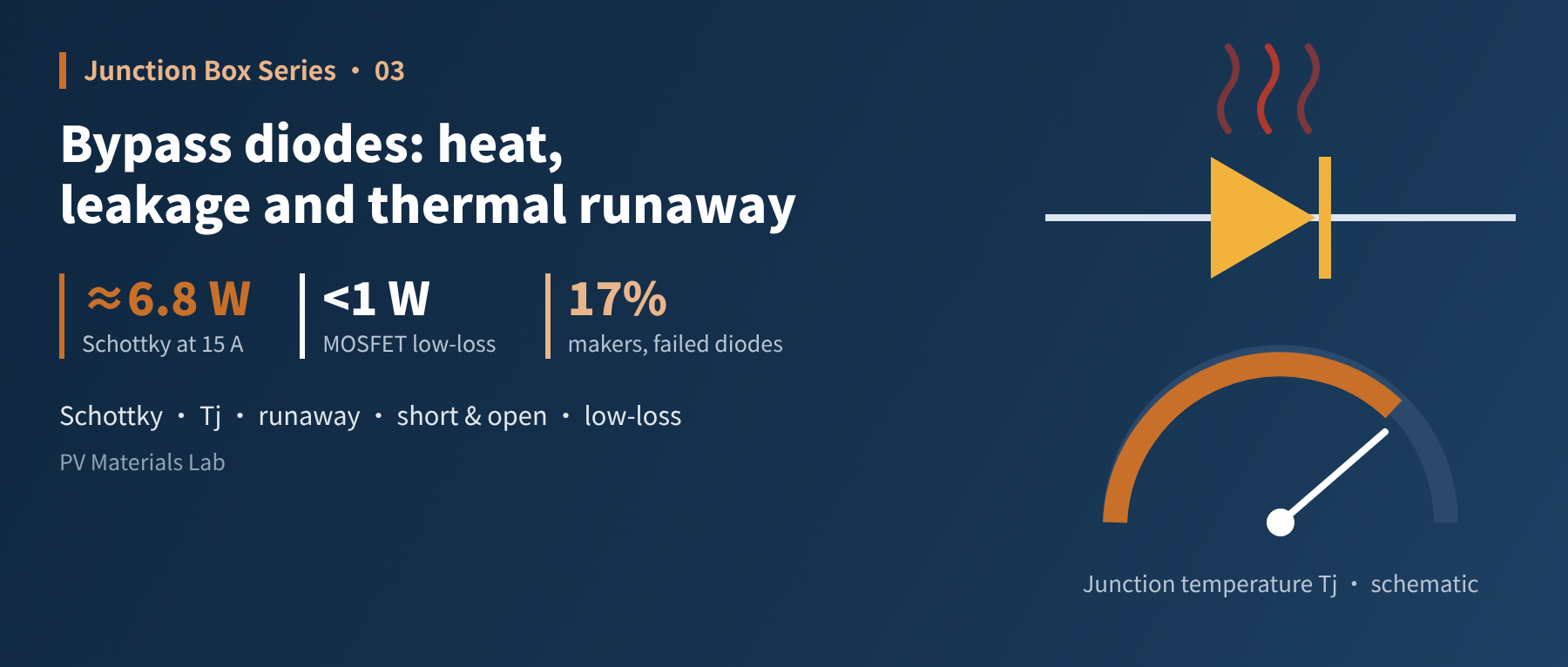
Conducting generates heat, blocking leaks current, and at high temperature thermal runaway can follow — a complete look at how bypass diodes work, how they fail, and three ways forward in the high-current era. This is the third article of our junction box series (fundamentals: bypass diodes).
The previous two articles kept returning to one conclusion: in junction box design, heat dissipation is the main thread. And the source of that thread is the small bypass diode.
It is idle most of the time, but when it works it is the biggest heat source in the box; when it fails it does so silently, yet the module loses a third of its power outright — or even its hot-spot protection.
This article is devoted to it: Why does it generate heat? Why can thermal runaway happen? What should be done in the high-current era?
01Two states, both generating heat
A bypass diode has only two operating states: forward conduction and reverse blocking. Many people focus only on the heat when conducting, but the blocking state also dissipates power — it is just usually small enough to ignore.
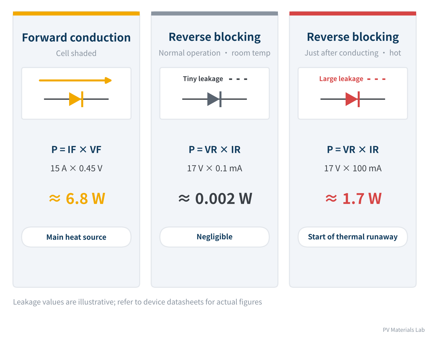
Figure 1 Three operating conditions of a diode and their heat generation
- Forward conduction: When a cell is shaded, the diode carries a current close to the module's short-circuit current, and the heat equals current times forward voltage. This is the largest heat source.
- Reverse blocking · room temperature: During normal generation the diode sees the substring voltage with only a tiny leakage current, and dissipation is negligible.
- Reverse blocking · high temperature: Right after conduction ends, while the chip is still very hot, leakage can be hundreds or thousands of times higher, and dissipation is no longer negligible.
The third condition is the most easily overlooked, yet it is exactly where thermal runaway begins. Keep it in mind; we will come back to it.
02Why Schottky?
The advantages and drawbacks of Schottky diodes stem from the same physical root: a low barrier.
A standard diode is a PN junction; a Schottky diode is a junction formed by contact between metal and semiconductor. Its barrier is lower, so:
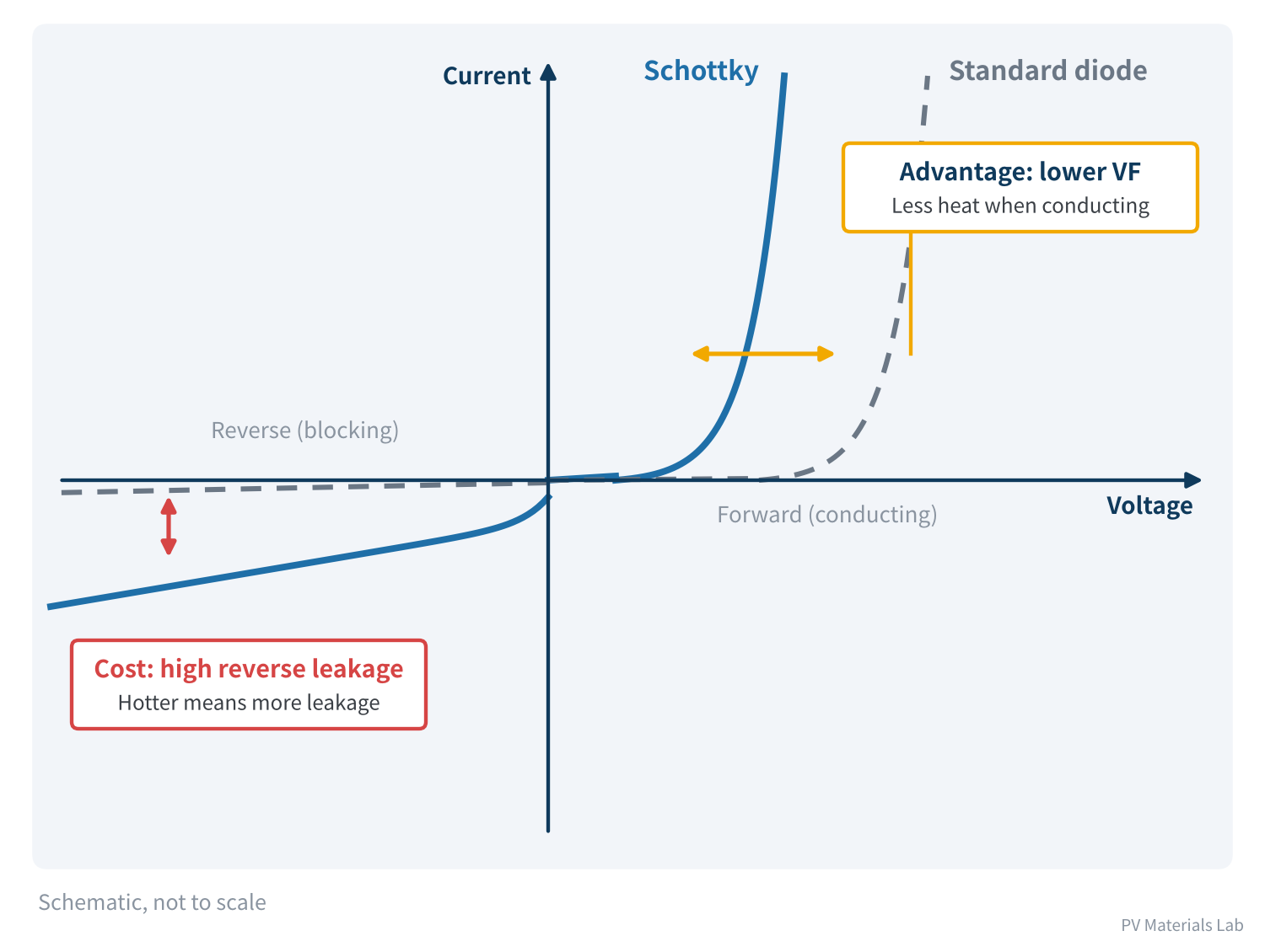
Figure 2 Characteristics of Schottky vs standard diodes
- Low forward voltage: About 0.3–0.5 V for Schottky versus about 0.7–1.0 V for standard diodes. At the same current, heat is roughly halved.
- High reverse leakage: Several orders of magnitude higher than standard diodes, and rising roughly exponentially with temperature — as a rule of thumb, doubling about every 10 °C (refer to the device datasheet).
For bypass diodes, conduction heat is the primary concern, so the industry chose Schottky diodes and accepted the price of high leakage. Almost all the trouble that follows comes from this price.
Worse, within the same type of device the two parameters pull against each other: the lower the forward voltage, the higher the leakage tends to be. Selecting on forward voltage alone plants a mine for thermal runaway.
03Reading the datasheet: junction temperature is the core
All diode parameters ultimately come down to one quantity: junction temperature Tj, the actual temperature inside the chip. It cannot be measured directly; in engineering practice it is often estimated from case temperature:
Tj = Tc + P × Rth(j-c)
Tc: case temperature, measured with a thermocouple on the diode case;
P: diode heat dissipation, equal to current times voltage drop when conducting;
Rth(j-c): junction-to-case thermal resistance, set by the package and given in the datasheet.
Suppose a test measures a case temperature of 150 °C, a current of 15 A, a forward voltage of 0.40 V at high temperature and a junction-to-case thermal resistance of 2 °C/W:
Heat P = 15 × 0.40 = 6 W;
Junction temperature Tj = 150 + 6 × 2 = 162 °C.
If the device's maximum junction temperature is 200 °C, 38 °C of margin remains; if it is 175 °C, only 13 °C remains.
The formula points to three ways of lowering junction temperature:
| Approach | Term in the formula | What to do |
|---|---|---|
| Lower case temperature | Tc | Larger copper terminals, thermally conductive potting, split structure |
| Lower heat generation | P | Devices with lower voltage drop, or a low-loss solution |
| Lower thermal resistance | Rth(j-c) | Move from axial to SMD or module packages |
Table 1 Three ways to lower junction temperature
First, rated current is usually specified at a given case temperature; the higher the temperature, the lower the allowed current, so check the derating curve rather than just the nominal value. Second, forward voltage falls and leakage rises with temperature, so good room-temperature data do not mean safety at high temperature.
04How standards test it
Standards contain two dedicated tests for bypass diodes, answering "can it survive conduction?" and "does it stay stable when switched back to blocking?"
IEC 61215: bypass diode test (MQT 18)
- Thermal test (MQT 18.1): First, the relationship between diode forward voltage and junction temperature is calibrated with pulsed current at 30, 50, 70 and 90 °C. The module is then heated to 75 ± 5 °C and a forward current equal to the STC short-circuit current is applied for 1 hour; the junction temperature is derived from the measured forward voltage and must not exceed the diode manufacturer's maximum junction temperature rating. The current is then raised to 1.25 times the short-circuit current for another hour, after which the diode must still work.
- Functionality test (MQT 18.2): Verifies that after the thermal test and other stress tests the diode still conducts normally and has not gone open-circuit.
Note that the current IEC 61215-2:2021 derives junction temperature by the forward-voltage calibration method rather than measuring case temperature directly; the case-temperature formula in the previous section is better suited to engineering estimates and design checks. IEC 62790:2020 also added a bypass diode thermal test and a reverse overload current test at junction-box level.
IEC 62979: thermal runaway test
This test simulates exactly the scenario of "shading suddenly clearing": at high temperature the diode is first forward-biased and allowed to heat up fully, then quickly switched to reverse bias, and its temperature is watched to see whether it gradually falls or keeps rising. If it keeps rising, that is thermal runaway. The standard is aimed mainly at Schottky diodes; PN-junction diodes are exempt.
The two tests examine different things. Passing the thermal test does not mean thermal runaway cannot happen — the former looks at junction temperature while conducting, the latter at stability after switching back to blocking.
05Thermal runaway: the most hidden killer
Now back to the question left open in Section 01. What happens the moment shading clears?
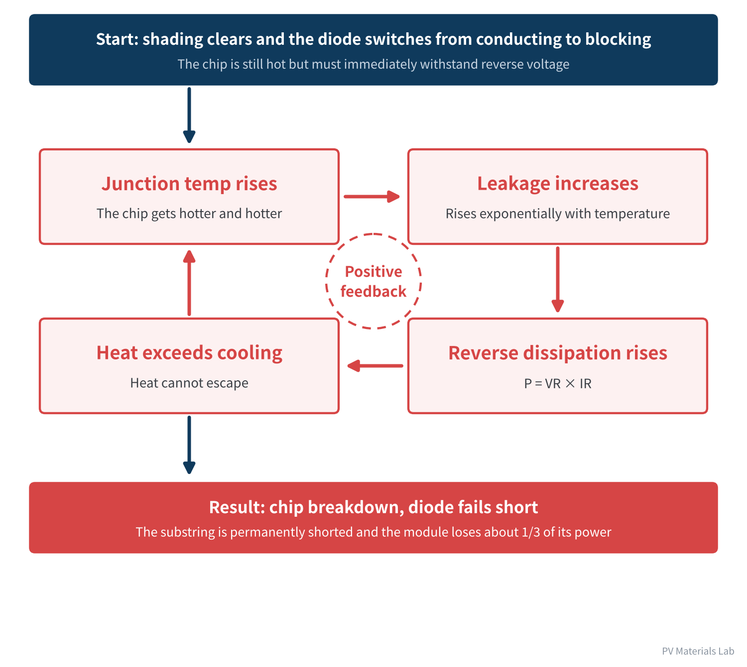
Figure 3 Thermal runaway: a self-accelerating positive feedback loop
The diode has just stopped conducting and the chip may still be above 150 °C when the substring voltage is reapplied across it. Leakage is high at this point, and so is reverse dissipation. If this heat exceeds what the junction box can dissipate, the chip temperature rises instead of falling, leakage increases further — and a self-accelerating positive feedback loop forms until the chip breaks down.
Whether it runs away depends on a race
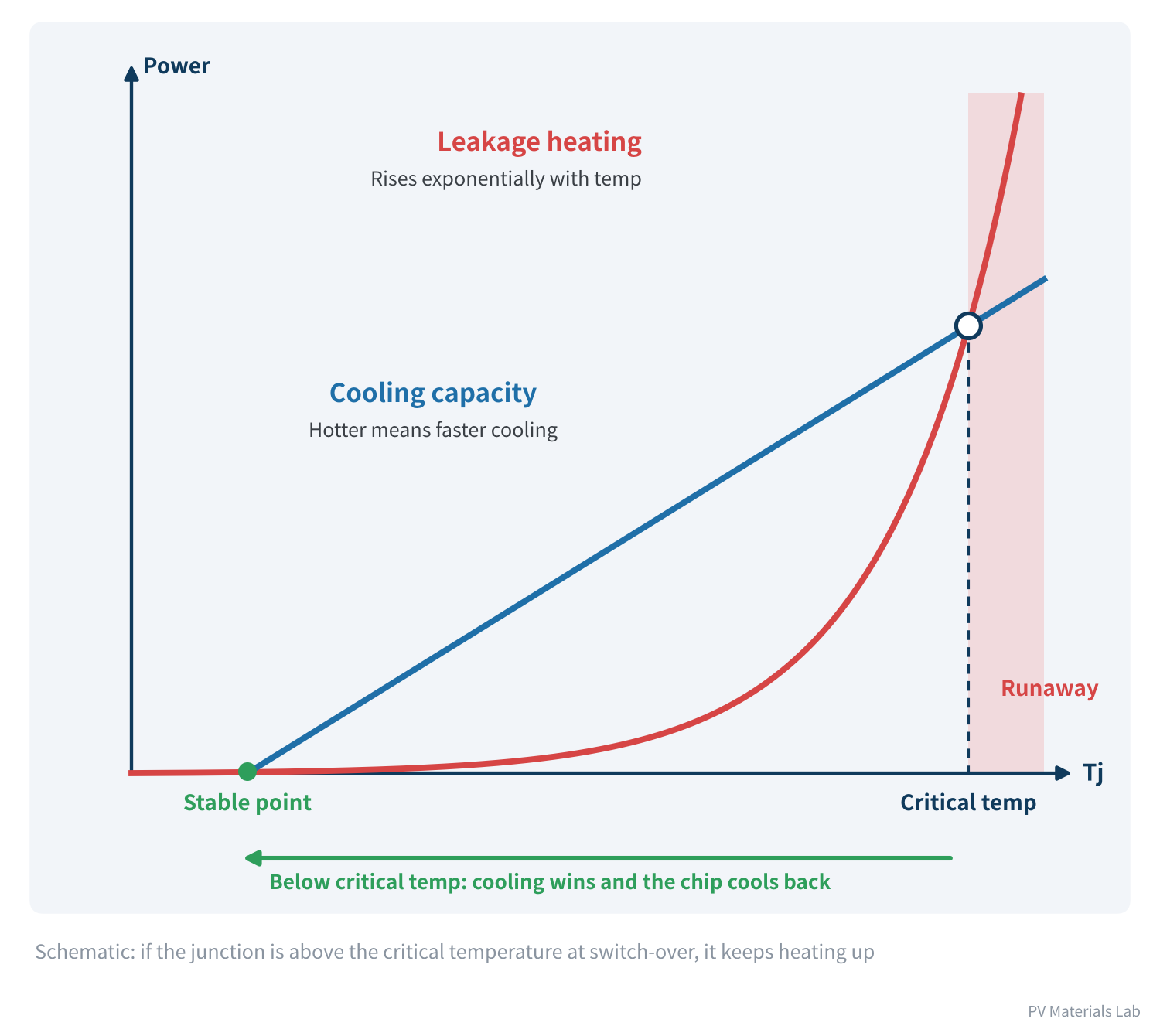
Figure 4 A race between heating and cooling: the critical temperature
Plot "leakage heating" and "cooling capacity" on the same chart and the race becomes clear:
- Two curves: Cooling capacity rises roughly linearly with temperature; leakage heating rises exponentially.
- Critical temperature: The upper crossing point of the two lines defines a critical temperature. Below it, cooling wins and the chip slowly cools back to the stable point; above it, heating wins and the temperature keeps climbing.
- What matters: Which side of the critical temperature the junction is on at the moment of switching back to blocking.
When runaway is more likely
| Factor | Effect | Typical scenario |
|---|---|---|
| High device leakage | Raises the heating curve and lowers the critical temperature | Devices chosen purely for low forward voltage |
| Poor heat dissipation | Flattens the cooling line and lowers the critical temperature | Small box, thin copper, low-conductivity potting |
| High ambient temperature | Shifts the cooling line right, reducing margin | Rooftops, BIPV, hot regions |
| High reverse voltage | More heat for the same leakage | Layouts with many cells per substring |
Table 2 Conditions that make thermal runaway more likely
Thermal runaway is hidden because it happens not during shading but after shading ends; not in a room-temperature lab, but on a rooftop at noon in summer.
06Two failure modes
Bypass diode failures ultimately take two forms:
| Item | Short-circuit failure | Open-circuit failure |
|---|---|---|
| Common causes | Thermal runaway, overheating breakdown, ESD or lightning surge | Detached solder joints, broken leads, burnt out by overcurrent |
| Normal behaviour | The substring is shorted; module power and open-circuit voltage each drop by about 1/3 | Nothing abnormal |
| Hidden risk | Substring current keeps flowing through the damaged diode, heating the box long-term | Once shading occurs, hot spots are unprotected |
| Detection | Open-circuit voltage, I-V curve, IR thermography | Hard to find with routine checks; needs a dedicated functionality test |
Table 3 The two failure modes of bypass diodes
Short-circuit failures are visible and cost energy yield; open-circuit failures are invisible and plant a safety hazard. The latter deserves more vigilance.
Third-party data show this is not a rare problem. Kiwa PVEL's 2026 Reliability Scorecard reports that 17% of participating manufacturers had at least one failed bypass diode in the past year, and 21% had a junction-box-related failure; the lab checks diode function after thermal cycling and mechanical stress sequences, and the scorecard records a case of the diode/junction box melting due to a short circuit after only TC200.
Schottky diodes are relatively sensitive to electrostatic discharge and voltage surges. Inadequate ESD protection in production, or induced overvoltage from lightning at the plant, can damage the chip. Such damage sometimes does not cause immediate failure but shows up as higher leakage — pushing the device towards the edge of thermal runaway ahead of time.
07Three ways forward in the high-current era
Module currents have gone from 9 A to 15 A, 18 A and beyond, and bifacial modules add rear-side gain. Conduction heat is proportional to current, so the pressure on bypass diodes only grows. The industry's responses fall roughly into three routes.
Route 1: better Schottky diodes
At chip level, trench Schottky structures control leakage better at lower forward voltage; at package level, moving from SMD to module packages places the chip directly on a large copper lead frame, lowering junction-to-case thermal resistance. This is the lowest-cost route and currently the mainstream.
Route 2: stronger heat dissipation
The structural and material choices covered in the previous article — split layouts, larger and thicker copper terminals, higher-conductivity potting — all lower case temperature. They do not change the amount of heat generated, but remove it faster.
Route 3: a different device
Replacing the diode with a MOSFET plus control circuit reduces heat at the root. A conducting MOSFET acts like a milliohm-level resistor; at 4 mΩ and 15 A, the voltage drop is only about 60 mV.
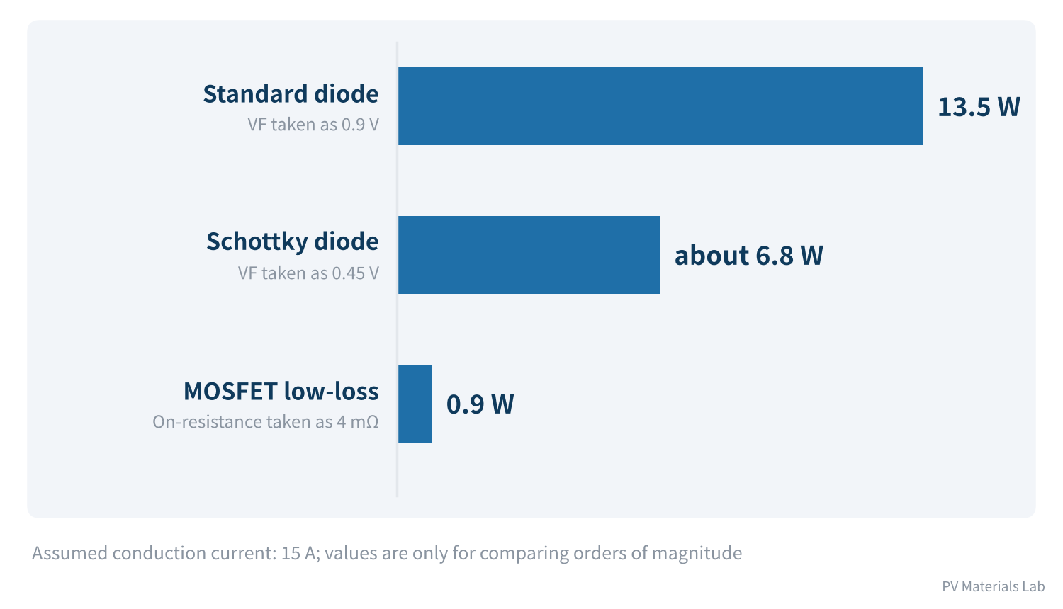
Figure 5 Conduction heat of three bypass solutions
At 15 A, a Schottky diode generates about 6.8 W while a MOSFET solution generates under 1 W — nearly an order of magnitude less. It also lacks the Schottky's high-temperature leakage problem, so the risk of thermal runaway is much lower.
But it is not free:
- Higher cost: One diode becomes a whole circuit.
- Higher complexity: Extra control chips and peripheral components each add a new failure point that must survive 25+ years outdoors.
- Less track record: Compared with Schottky diodes used for decades, long-term reliability data are still limited.
| Item | Schottky (module package) | MOSFET low-loss solution |
|---|---|---|
| Conduction heat | Higher | An order of magnitude lower |
| High-temperature leakage | Significant; thermal runaway risk | Very small |
| Cost | Low | High |
| Circuit complexity | Single device | Device + control circuit |
| Maturity | Mainstream | Being introduced gradually, mostly in smart junction boxes |
Table 4 Schottky vs MOSFET low-loss solutions
For now the mainstream remains a combination of the first two routes: better Schottky diodes plus stronger heat dissipation. The third route is worth watching as currents keep rising and costs fall.
08Six recommendations for selection and incoming inspection
- Evaluate together: Alongside forward voltage, always check the leakage curve at high temperature, and assess the two together.
- Use derating: Check rated current against the high-temperature derating curve, not the room-temperature nominal value.
- Leave margin: Keep ample junction temperature margin, calculated for the layout with the highest short-circuit current; for bifacial modules, include rear-side gain.
- Run both tests: Run both the thermal test and the thermal runaway test, using the worst combination: the highest-current layout with the worst-cooling box.
- Look at distributions: Watch batch consistency by sampling the distribution of forward voltage and leakage, not just the average.
- ESD control: Enforce ESD protection throughout production, and monitor abnormal leakage in incoming and in-process inspection.
09Final thoughts
1. Bypass diodes generate heat both when conducting and when blocking; reverse leakage at high temperature is the easily overlooked part.
2. Schottky diodes are chosen for low forward voltage at the price of high leakage; the two parameters pull against each other and must be considered together.
3. All parameters come down to junction temperature; lowering case temperature, heat generation and thermal resistance are the three routes.
4. Thermal runaway happens after shading ends and depends on whether the junction is above the critical temperature when switching back to blocking.
5. Open-circuit failure is more hidden and more dangerous than short-circuit failure.
6. Ways forward in the high-current era: better Schottky diodes, stronger heat dissipation and low-loss MOSFET solutions.
One diode drives the thermal design of the whole junction box. Understand it, and many junction box design choices follow naturally.
In the next article, Junction Box Series 4 covers connectors and cables: contact resistance, cross-mating risks and crimp quality — where the hot spots for plant fires really are.
What pitfalls have you met in bypass diode selection or failure analysis? We would be glad to hear from you.
References
- IEC 61215-2:2021 Terrestrial photovoltaic (PV) modules – Design qualification and type approval – Part 2: Test procedures (MQT 18 bypass diode test)
- IEC 62979:2017 Photovoltaic modules – Bypass diode – Thermal runaway test
- IEC 62790:2020 Junction boxes for photovoltaic modules – Safety requirements and tests
- Sinovoltaics: IEC 61215 MQT 18: Bypass Diode Testing for Solar Modules, https://sinovoltaics.com/learning-center/testing/iec-61215-mqt-18-bypass-diode-testing-for-solar-modules/
- Kiwa PVEL: 2026 PV Module Reliability Scorecard – Failures, https://2026scorecardsbx.pvel.com/failure
- TÜV Rheinland: Update on standard: revised junction box standard IEC 62790:2020, https://insights.tuv.com/blog/update-on-standard-revised-junction-box-standard-iec-627902020
A PV R&D and technology team with 10+ years of experience | In-depth technical knowledge sharing
Materials · Reliability · Failure Analysis · Standards & Certification · Products · Processes
Exploring AI + PV; collaboration welcome
Disclaimer:
1. Original content reflects the authors' personal views only, is for reference only and does not constitute investment advice.
2. Reposted and cited content is credited to its source, out of respect for original work.
3. Some content was produced with AI assistance (chart generation, data retrieval, concept explanations, etc.); the core framework and key content were written by our technical team and reviewed by people.
4. If anything is inaccurate or infringes your rights, please leave a message or contact us and we will deal with it.