
Junction Box Series 2 | Inside a Junction Box: Structure, Types and Materials Explained
In brief
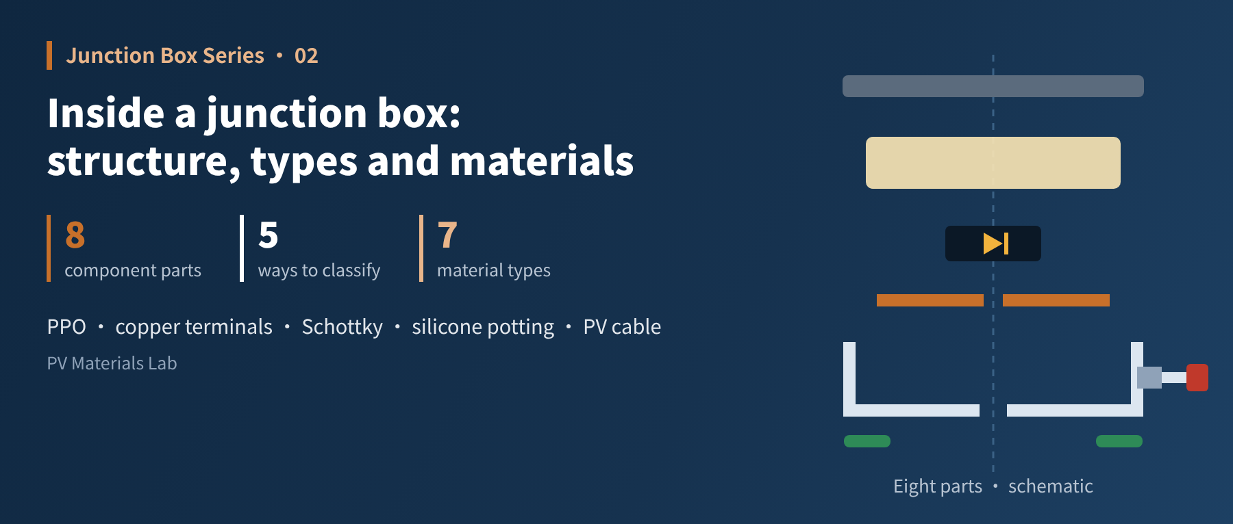
Eight parts, five ways to classify, seven types of material — we take a junction box apart to understand the selection logic behind every material. This second article of our junction box series (fundamentals) builds on the "three functions" of the first and answers three questions: what is it made of, how are products classified, and why is each material chosen?
In the previous article we covered the three functions of a junction box: current output, bypass protection, and sealing and insulation.
Functions are "what it must do"; structure and materials are "how it does it". Boxes that all go by the name junction box — one-piece or split, potted or non-potted, axial or module diodes — embody completely different design trade-offs.
In this article we take a junction box apart and answer three questions: What is it made of? How are products classified? Why is each material chosen?
01Taking it apart: eight components
Take a mainstream potted junction box apart from top to bottom and you get eight parts:
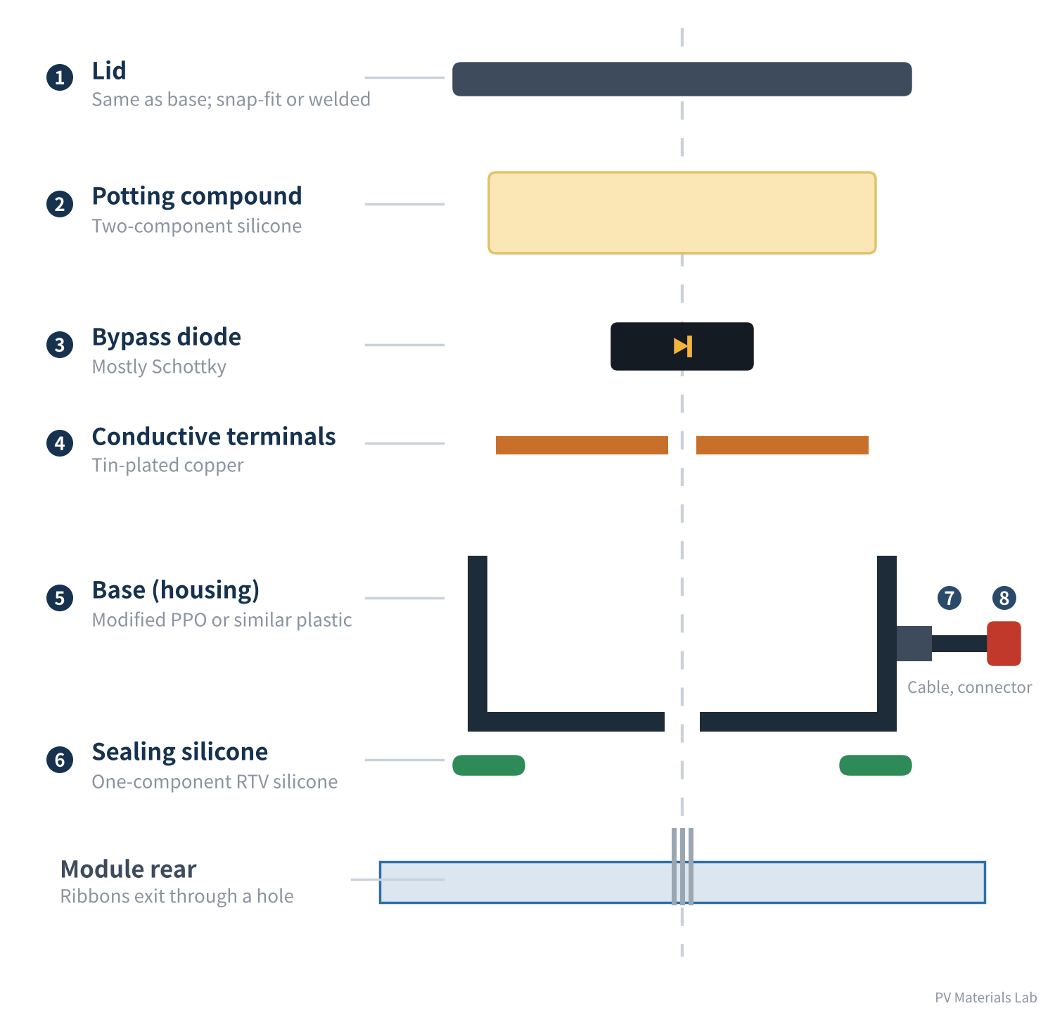
Figure 1 Inside a junction box: eight components
They fall into three groups that map neatly onto the three functions from the previous article:
- Conductive path: Conductive terminals, cable and connector — responsible for current output.
- Protective device: Bypass diode — responsible for bypass protection.
- Protection system: Base, lid, potting compound and sealing silicone — responsible for sealing and insulation.
The conductive terminals and the potting compound each "wear several hats": the terminals conduct current and dissipate heat, while the potting compound seals, insulates and conducts heat. This point will come up again and again when we discuss materials.
02Classification: five dimensions that explain product differences
Supplier catalogues list many models, but the differences mainly come down to five dimensions:
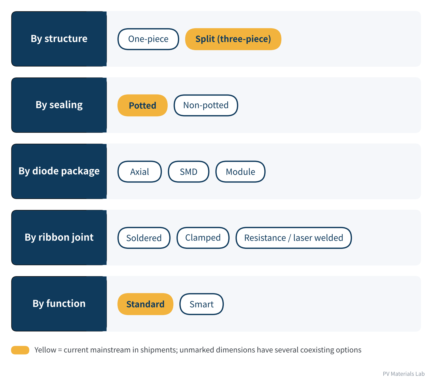
Figure 2 Five ways to classify junction boxes
By structure: one-piece vs split
As introduced in the previous article, a one-piece box houses three diodes in one enclosure, while a split (three-piece) design uses three small boxes with one diode each. With half-cut modules now mainstream, split boxes have become the bulk of shipments thanks to shorter wiring and distributed heat sources.
By sealing: potted vs non-potted
This is the most fundamental structural divide, deciding what the box relies on for water protection and insulation.
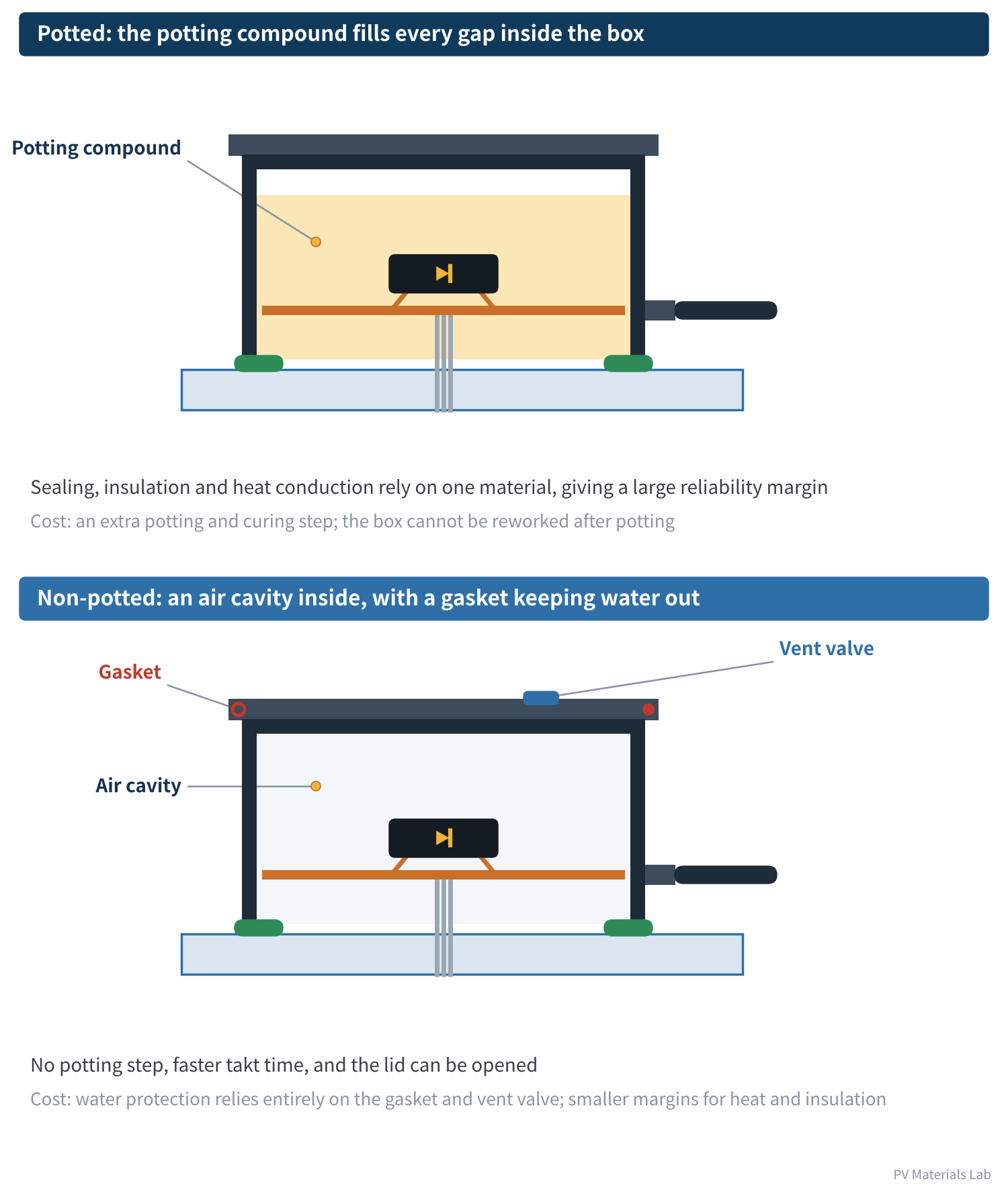
Figure 3 Cross-sections of potted and non-potted junction boxes
- Potted: The gaps inside the box are filled with potting compound, completely encasing live parts. Even if moisture gets past the first line of defence, it cannot reach the metal parts.
- Non-potted: An air cavity remains inside; water protection relies on the lid gasket, insulation relies on sufficient creepage and clearance distances, and a vent valve is usually added to balance internal and external pressure and reduce condensation.
Non-potted boxes skip the potting and curing steps, but place reliability on the long-term performance of the gasket and vent valve. Given high currents and long warranties, potted boxes are currently the mainstream choice.
By diode package: axial, SMD and module
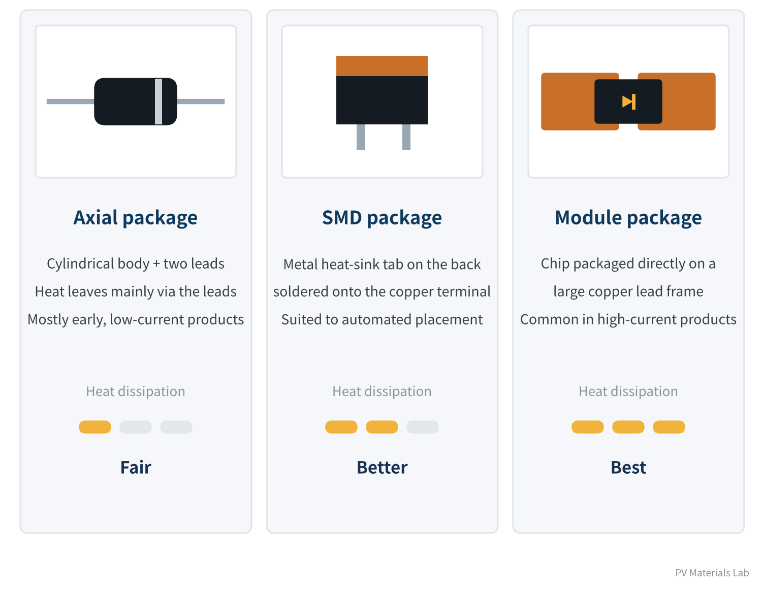
Figure 4 Three package types for bypass diodes
All three packages evolve in one direction: bring the chip closer to copper so heat can get out more easily. The higher the module current, the more this matters. Diode selection and failure mechanisms are covered in the next article.
By ribbon connection: soldering, clamping and resistance/laser welding
- Soldering: A mature process, but highly dependent on operator consistency; cold joints and flux residues are common hidden risks.
- Clamping: A spring clip holds the ribbon — no soldering and fast; contact pressure must be maintained by the spring over the long term, and stress relaxation of the metal is a risk that needs validation.
- Resistance / laser welding: No flux, easy to automate, consistent, but with higher equipment investment; the direction for automated lines.
By function: standard vs smart
Smart boxes integrate optimiser, shutdown or monitoring circuits on top of a standard junction box. Their structural and material requirements differ significantly from standard boxes, and will be covered in a later special topic.
03Materials: the selection logic behind seven material types
Junction box material selection is essentially solving a problem under three constraints — electrical, thermal and environmental — plus a cost constraint.
① Base and lid: modified PPO
The mainstream housing material is modified PPO (polyphenylene oxide, also written PPE). It is chosen for a combination of properties:
- Low water absorption, hydrolysis resistance: Dimensions and insulation remain stable in damp heat. This is its main advantage over nylon (PA), whose dimensions and electrical properties change after absorbing water.
- Good electrical insulation: And halogen-free flame retardancy is easy to achieve.
- High heat rating: It withstands diode operating temperatures over the long term.
Four indicators are used to evaluate a housing material:
| Indicator | Meaning | Why it matters |
|---|---|---|
| Flammability rating | UL 94 rating | Must not support combustion if the inside overheats |
| RTI | Relative temperature index | Upper limit for long-term operating temperature |
| CTI | Comparative tracking index | Determines the material group, which affects creepage distance design |
| Outdoor suitability | Property retention after UV and water immersion ageing | Basic threshold for 25 years outdoors |
Table 1 Four indicators for evaluating housing materials
CTI is more than a material parameter. Under IEC 60664-1, CTI ≥ 600 is material group I, 400–600 group II, 175–400 group IIIa and 100–175 group IIIb. The higher the CTI, the better the material group and the smaller the creepage distance the standard requires at the same voltage — which is what makes a more compact box possible.
② Conductive terminals: tin-plated copper
The conductive terminals are both conductor and heat sink, so there is only one direction for the material: copper.
- Pure copper: Best electrical and thermal conductivity; the first choice for high-current products.
- Brass: Strong, easy to stamp and low-cost, but with only about 30% of the conductivity of pure copper (about 28% IACS).
The surface is usually tin-plated to prevent copper oxidation and ensure solderability to ribbons and diodes. Terminal thickness and area directly determine heat dissipation, which makes this the place most often cut during "cost reduction" — and the place that should least readily be cut.
③ Bypass diode: mostly Schottky
Bypass diodes are mostly Schottky diodes, because their low forward voltage means less heat when conducting. Five parameters guide selection:
| Parameter | Meaning | Selection direction |
|---|---|---|
| Rated current IF | Forward current it can carry long-term | Must cover module short-circuit current with margin |
| Reverse voltage VR | Voltage it withstands when blocking | Higher than the open-circuit voltage of one substring |
| Forward voltage VF | Voltage drop when conducting | Lower means less conduction heat |
| Reverse leakage IR | Leakage current when blocking | The smaller the better, especially at high temperature |
| Max junction temperature Tj | Highest temperature the chip may reach | Higher means more thermal design margin |
Table 2 Five selection parameters for bypass diodes
The reverse voltage across one diode is roughly the open-circuit voltage of the substring it protects — about one third of the module's open-circuit voltage. For a module with an open-circuit voltage of about 52 V: 52 ÷ 3 ≈ 17 V. Allowing for the rise in open-circuit voltage at low temperature — with a typical TOPCon open-circuit voltage temperature coefficient of about −0.25%/°C, the open-circuit voltage at −25 °C is about 12.5% higher — one substring reaches about 19.5 V. The common 40–50 V Schottky diodes therefore already have ample voltage margin. What is really tight is not voltage but current and heat dissipation.
There is a built-in conflict: the lower the forward voltage, the higher the reverse leakage tends to be, and the greater the risk of thermal runaway at high temperature. VF and IR must be considered together. This is one reason IEC 62790:2020 added a bypass diode thermal test and a reverse overload current test — the standard now examines diodes more directly under the real thermal conditions inside a junction box.
④ Potting compound: two-component silicone
The potting compound must seal, insulate, conduct heat and retard flame all at once; the mainstream choice is two-component silicone potting compound. By curing mechanism there are two types:
| Item | Condensation cure | Addition cure |
|---|---|---|
| Curing | Room temperature, needs moisture | Platinum-catalysed, can be heat-accelerated |
| By-products | Releases small molecules | None |
| Deep curing | Slower, from the surface inward | Uniform throughout |
| Adhesion | Better adhesion to substrates | Relatively weaker, often needs a primer |
| Main risk | Incomplete cure in thick sections | Catalyst "poisoning" leading to no cure |
Table 3 Condensation-cure vs addition-cure silicone potting compounds
Key indicators include thermal conductivity, flammability rating, volume resistivity, adhesion to housing and cable, and process parameters such as viscosity and pot life.
The platinum catalyst in addition-cure silicone is deactivated by compounds containing sulphur, phosphorus or nitrogen, or by organotin, showing up as a tacky interface or no cure. Flux residues and the organotin catalyst in condensation-cure silicone are common "poisons". Compatibility must be validated before changing compounds.
⑤ Sealing silicone: one-component RTV
The box is bonded to the module rear with a one-component room-temperature-vulcanising silicone sealant. It cures from the surface inward by absorbing moisture from the air, so after dispensing it needs curing time before handling and testing.
Its key test is adhesion: bond strength at both interfaces — to the backsheet or glass and to the housing — and its retention after damp heat, UV and thermal cycling ageing. Most cases of junction boxes detaching or water entering at the interface originate in this layer.
⑥ Cable: tinned copper + crosslinked polyolefin
- Conductor: Stranded tinned copper, flexible and corrosion-resistant. The mainstream cross-section is 4 mm², with 6 mm² used for high-current products.
- Insulation and sheath: Irradiation-crosslinked halogen-free low-smoke polyolefin in a double-layer structure, resistant to UV, ozone and temperature extremes.
- Rated voltage: DC 1,500 V, under IEC 62930 and EN 50618.
⑦ Connector: a combination of three materials
- Contacts: Tin- or silver-plated copper alloy with a multi-point contact design for low, stable contact resistance.
- Housing: Modified PPO or nylon, with requirements similar to the junction box housing.
- Seal: Silicone rubber or similar elastomer to ensure the ingress protection rating when mated.
Small as it is, the connector is the only electrical connection in the whole system made by "plugging in", and is covered by IEC 62852. It deserves an article of its own.
One new trend worth watching is higher system voltage: in 2026 connector makers already offer DC 2,000 V PV connectors certified to UL 6703 (such as Amphenol's H4 P2KV). Once 2,000 V systems spread, the creepage and insulation design of cables, connectors and even junction boxes will need upgrading, and the value of CTI and material groups will become even more apparent.
04The underlying logic of material selection: heat is the main thread
Look at the seven material types together and one thread runs through them all: heat dissipation.
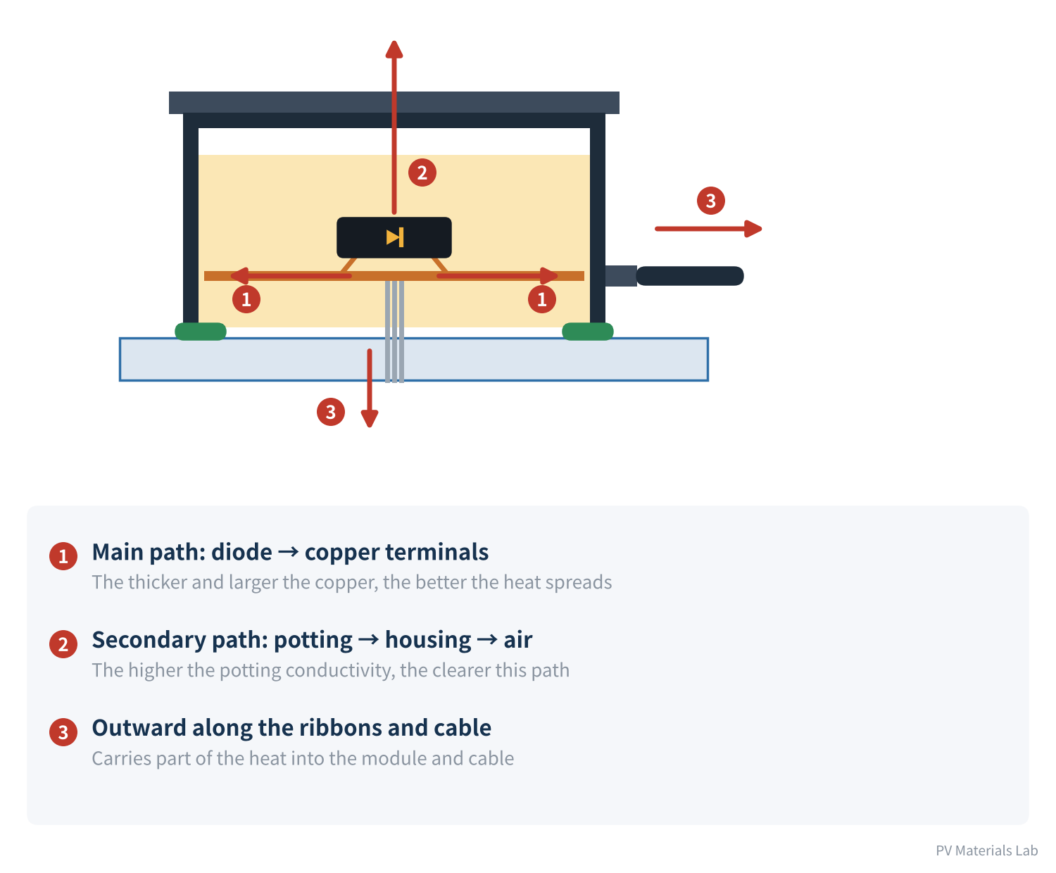
Figure 5 Where the diode's heat goes
Copper's thermal conductivity is about 400 W/(m·K), while potting compound is usually below 1 W/(m·K) and housing plastics are lower still — a difference of several hundred times. So most of the diode's heat first spreads sideways along the copper terminals, then passes through the potting compound and housing into the air.
This explains several earlier choices:
- Packages: Diode packages move from axial to SMD and module types — to lower the thermal resistance between chip and copper.
- Terminals: Terminals use pure copper and are made thicker and larger — to spread the heat.
- Potting: Potting compounds aim for higher thermal conductivity — to open up the last stretch.
- Structure: One-piece boxes give way to split boxes — so that the three heat sources no longer "bake" each other.
Another hidden thread: compatibility between materials
Many materials work side by side in a junction box for decades. Each material passing on its own does not mean the combination is trouble-free:
- Cure inhibition: Potting compound may be inhibited by flux residues or sealant.
- Interface adhesion: Poor adhesion between potting compound and housing or cable sheath turns the interface into a path for moisture.
- Corrosion: Long-term contact between metal parts and adhesive by-products or residues can cause corrosion.
So a junction box material change is never as simple as "switching to another grade"; it must be revalidated within the whole system.
05The seven materials at a glance
| Component | Mainstream material | Key indicators |
|---|---|---|
| Base / lid | Modified PPO | Flame retardancy, RTI, CTI, weathering |
| Conductive terminals | Pure copper or brass, tin-plated | Conductivity, thickness, plating |
| Bypass diode | Schottky diode | IF, VF, IR, Tj |
| Potting compound | Two-component silicone | Thermal conductivity, flame retardancy, insulation, adhesion |
| Sealing silicone | One-component silicone sealant | Bond strength, cure speed, ageing resistance |
| Cable | Tinned copper + crosslinked polyolefin | Cross-section, voltage rating, weathering |
| Connector | Plated copper alloy + PPO / nylon | Contact resistance, ingress protection |
Table 4 The seven junction box materials at a glance
06Final thoughts
1. A junction box consists of eight parts in three groups: conductive path, protective device and protection system.
2. Product differences come from five dimensions: structure, sealing, diode package, ribbon connection and function.
3. The current mainstream is split + potted, with diode packages moving towards SMD and module types.
4. Selection of the seven materials revolves around electrical, thermal and environmental constraints, with heat dissipation as the main thread.
5. Compatibility between materials matters as much as the performance of each material; any change must be validated within the system.
Once you understand the structure and materials, you will find that most junction box failure cases can be traced back to a particular material or interface.
In the next article, Junction Box Series 3 turns to bypass diodes: comparing Schottky, module and low-loss solutions, and the mechanisms of junction temperature, leakage current and thermal runaway.
What problems have you met in junction box material selection or changes? We would be glad to hear from you.
References
- IEC 62790:2020 Junction boxes for photovoltaic modules – Safety requirements and tests
- IEC 62852 Connectors for DC-application in photovoltaic systems – Safety requirements and tests
- IEC 62930 / EN 50618 Electric cables for photovoltaic systems
- UL 94 Standard for Tests for Flammability of Plastic Materials
- IEC 60112 Method for the determination of the proof and the comparative tracking indices of solid insulating materials
- IEC 60664-1 Insulation coordination for equipment within low-voltage supply systems – Part 1: Principles, requirements and tests
- TÜV Rheinland: Update on standard: revised junction box standard IEC 62790:2020, https://insights.tuv.com/blog/update-on-standard-revised-junction-box-standard-iec-627902020
- Amphenol Industrial: H4 P2KV Solar Connector (DC 2,000 V, UL 6703), https://amphenol-industrial.com/?p=7256
A PV R&D and technology team with 10+ years of experience | In-depth technical knowledge sharing
Materials · Reliability · Failure Analysis · Standards & Certification · Products · Processes
Exploring AI + PV; collaboration welcome
Disclaimer:
1. Original content reflects the authors' personal views only, is for reference only and does not constitute investment advice.
2. Reposted and cited content is credited to its source, out of respect for original work.
3. Some content was produced with AI assistance (chart generation, data retrieval, concept explanations, etc.); the core framework and key content were written by our technical team and reviewed by people.
4. If anything is inaccurate or infringes your rights, please leave a message or contact us and we will deal with it.