
A Palm-Sized Box That Protects a Module for 25 Years: What a PV Junction Box Does
In brief
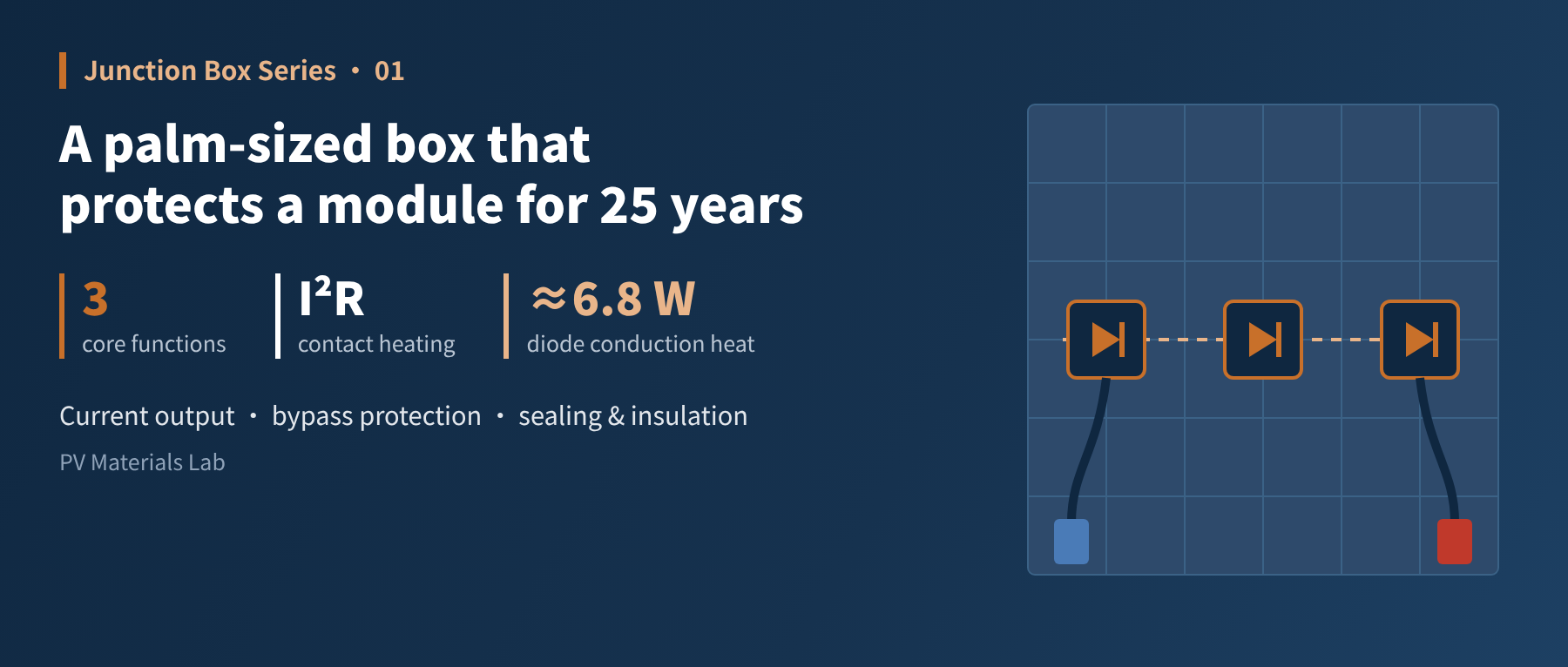
Current output, bypass protection, sealing and insulation: in this first article of our junction box series, we explain the three core functions of a PV junction box, the principle behind each, the key components and standard tests involved, and what goes wrong in the module, from heating and hot spots to leakage and even fire, when a function fails.
On a PV module, the glass and cells on the front attract almost all the attention. The palm-sized black box on the back, the junction box, is a small share of cost and has an even lower profile.
But anyone who has done plant O&M or failure analysis knows: many serious incidents, such as burnt-out modules and fires, happen at the junction box and connectors.
As the first article in our junction box series, we start with the most basic question: what does a junction box actually do?
01Meet the junction box
The junction box is bonded to the back of the module. The busbar ribbons of the cell strings come out through an opening in the backsheet (or rear glass) into the junction box, and then connect in series with neighbouring modules through two cables and a pair of positive and negative connectors.
Junction boxes come in two main forms:
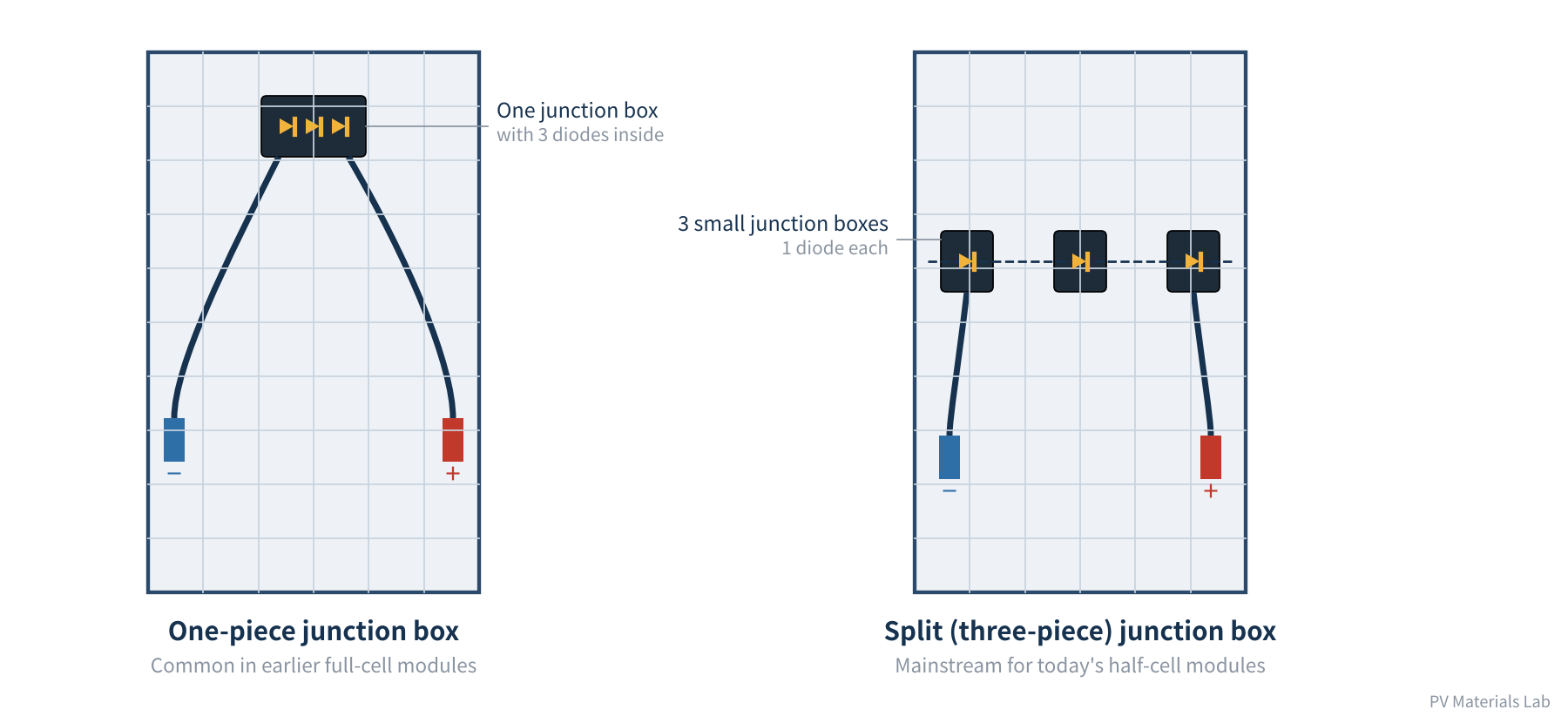
Figure 1 Location of the junction box on the module rear and its two common forms
- One-piece: a single box holding three bypass diodes, common in earlier full-cell modules and mounted at the top end of the module.
- Split (three-piece): divided into three small boxes with one diode each, mounted in the middle of the module; this is the mainstream solution for today's half-cell modules.
In half-cell modules the busbars exit from the middle of the module, so split junction boxes can "connect right where the busbars are", shortening busbars and internal wiring and lowering resistive losses; with the three diodes spread across three boxes, heat sources are no longer clustered and heat dissipation is better.
The forms keep changing, but the junction box always does the same three jobs:
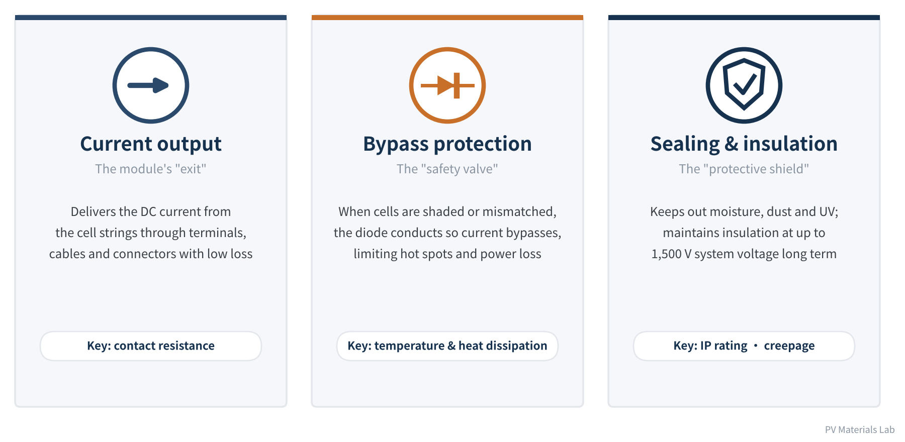
Figure 2 The three core functions of a junction box
02Function 1: Current output
The junction box is the module's "exit": every ampere the cells generate has to leave through it. The current path is: cell string → busbar → conductive terminal in the junction box → PV cable → connector → next module or inverter.
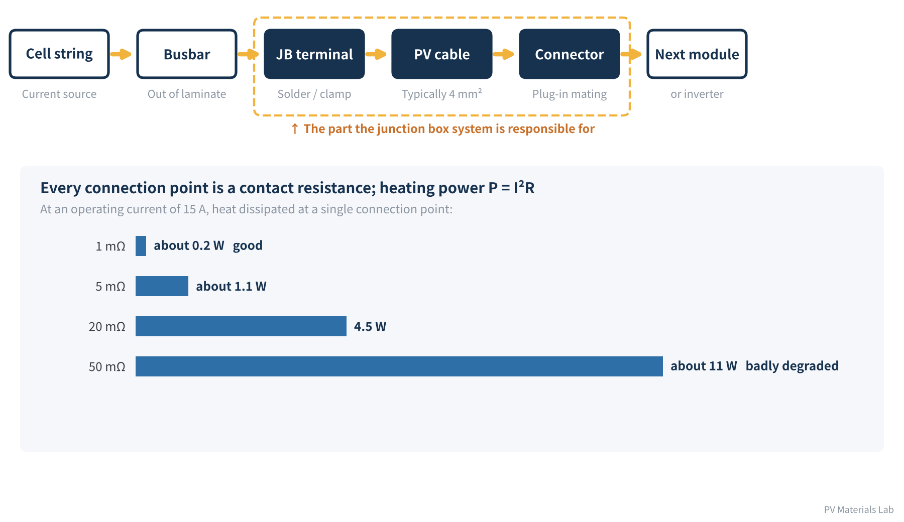
Figure 3 Current output path and heating from contact resistance
Every connection point along this path, whether the solder joint between busbar and terminal, the crimp between terminal and cable, or the mating point between male and female connectors, has contact resistance. Where there is resistance there is heat, and the heating power follows the simplest formula: P = I² × R.
Let's do the arithmetic at an operating current of 15 A:
- Contact resistance 1 mΩ: about 0.2 W of heat, negligible.
- Degraded to 20 mΩ: 4.5 W.
- Degraded to 50 mΩ: about 11 W, like putting a small soldering iron that never switches off inside a sealed little plastic box.
Worse, poor contact creates a vicious circle: heat → faster oxidation and material ageing → higher contact resistance → even more heat. Cold solder joints, poor crimps and connectors not fully mated all end the same way: a burnt box, or even arcing and fire.
Why is this becoming more important? Because module current keeps rising. Early modules with 156 mm cells had an operating current of only about 9 A; today modules with large 182 and 210 cells commonly reach 14–18 A or more, and bifacial modules add rear-side gain on top. Heating is proportional to the square of current: double the current and, with the same contact resistance, heating quadruples. That is why junction box current ratings have risen from 15 A in the past to 25 A and 30 A.
03Function 2: Bypass protection
The bypass diode is the module's "safety valve": idle most of the time, it opens a path for current when it matters.
How hot spots form. The cells in a module are connected in series, and in a series circuit the current is the same everywhere. When a cell is shaded by leaves, bird droppings, dust or the row in front, or has cracks or mismatch, it cannot produce as much current as the others. The other cells then "force" the same current through it, pushing it into reverse bias: instead of generating power it becomes a load, dissipating power from the other cells as heat. This is a hot spot. Its consequences range from significant local temperature rise to scorched and blistered backsheet, desoldered ribbon, shattered glass and, in severe cases, fire.
How the bypass diode steps in. The bypass diode is connected in anti-parallel across a cell substring and has two operating states:
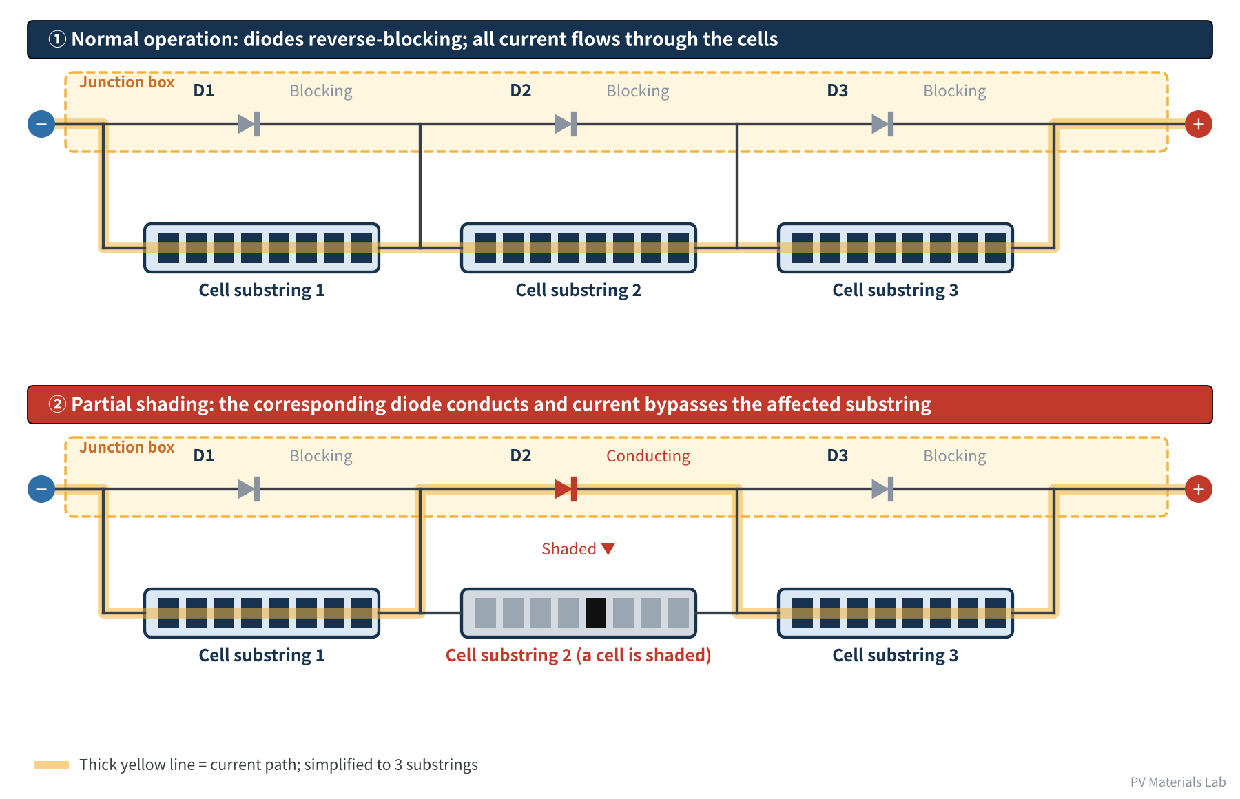
Figure 4 How a bypass diode works
- In normal operation: the voltage across the substring keeps the diode reverse-biased and blocking, with only a tiny reverse leakage current, as if it were not there.
- When shading occurs: the voltage across the affected substring reverses; once it exceeds the diode's forward voltage, the diode conducts and current bypasses that substring.
This has two effects:
- Limiting the hot spot: the reverse voltage across the shaded cell is limited to roughly "the sum of the voltages of the other cells in the same substring" (a dozen or so volts in mainstream half-cell modules), rather than the voltage of the whole string.
- Preserving energy yield: only the cells protected by that one diode are lost, about one third of the module; the rest keeps generating, and the current of the whole string is not dragged down by a single cell.
A bypass diode does not "eliminate" hot spots; it puts a "cap" on them. Whether the cell can withstand the capped condition must still be verified by the hot-spot endurance test in IEC 61215 (MQT 09).
The diode is a heat source too. Conducting is not free. Taking a Schottky diode's forward voltage of about 0.45 V, at 15 A one diode dissipates about 15 A × 0.45 V ≈ 6.8 W. Nearly 7 W concentrated in a fingernail-sized device, surrounded by a sealed plastic box and potting compound: if heat dissipation is inadequate and the diode's junction temperature exceeds its limit, performance degrades at best, and at worst the diode breaks down.
That is why the standards test it specifically:
- IEC 61215 bypass diode thermal test (MQT 18): at 75 °C ambient, a current equal to the short-circuit current Isc is applied for 1 hour, and the diode junction temperature must not exceed its rated limit; the current is then raised to 1.25 × Isc for another hour, after which the diode must still work.
- IEC 62979 bypass diode thermal runaway test: checks whether, when a hot diode switches from forward conduction back to reverse blocking, heating from reverse leakage current triggers a positive feedback loop of "hotter means more leakage, more leakage means hotter".
These tests are not overkill. Kiwa PVEL's 2026 reliability scorecard shows that 17% of participating manufacturers had at least one bypass diode failure (a non-functioning diode) in the past year, and one module developed a short circuit after only TC200 that melted the diode and junction box. Diode selection, heat dissipation and failure mechanisms deserve an article of their own, so we leave them for now.
04Function 3: Sealing and insulation
The junction box is the module's "protective shield", completely separating live parts from the outdoor environment and from people.
The inside of the junction box is one of the few places on a module with "exposed live metal", and it has to withstand 25–30 years of wind, sun and rain at DC system voltages of up to 1,500 V. Protection comes in layers:
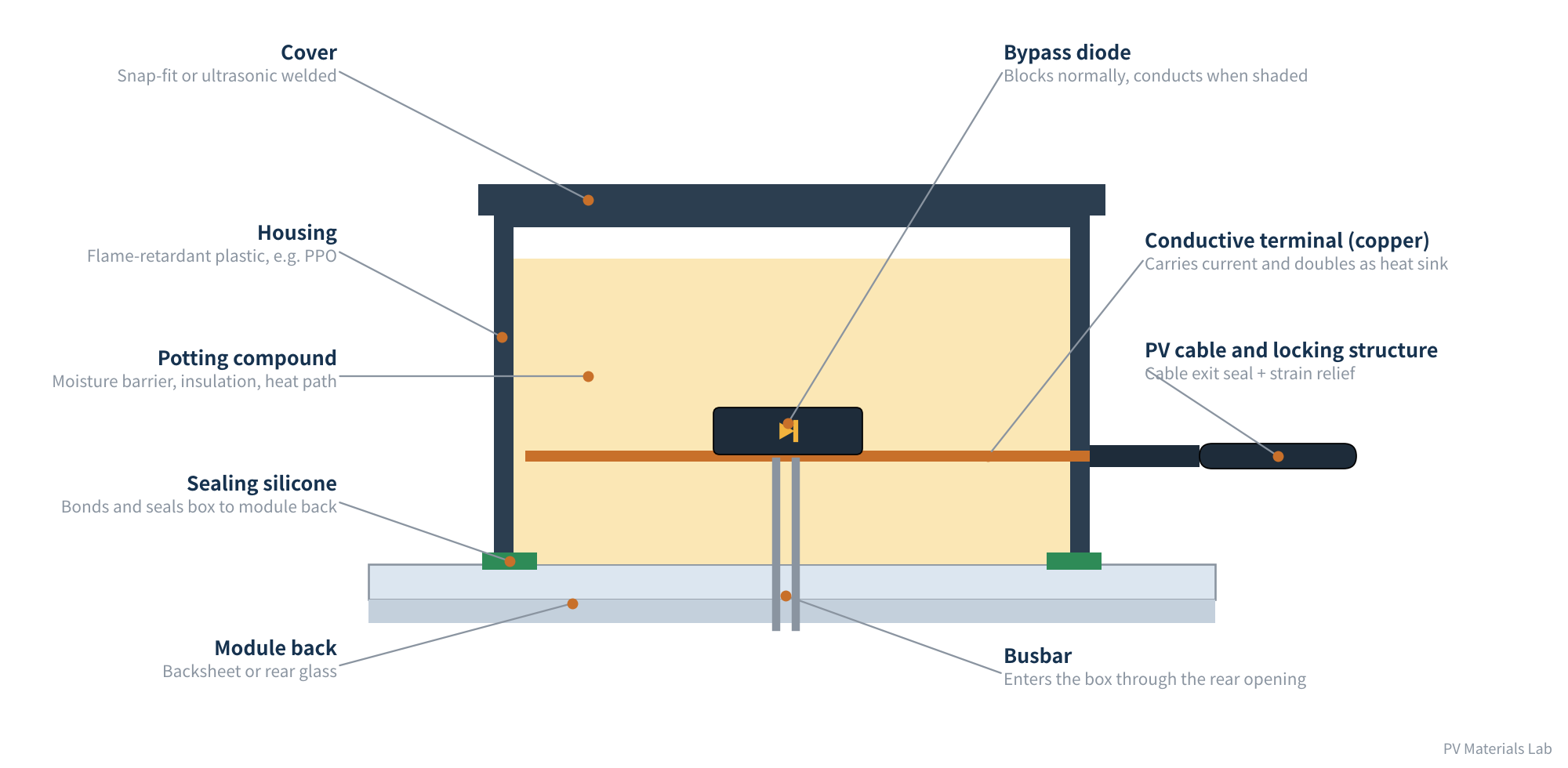
Figure 5 Junction box cross-section: layered sealing and insulation (schematic)
- Water and dust protection: sealing silicone bonds and seals the box to the module back, potting compound fills the space inside the box, and the cable exits have locking seal structures. Mainstream products are rated IP67 or IP68.
- Electrical insulation: there must be sufficient creepage and clearance distances between live parts and between live parts and outer surfaces, verified by tests such as insulation withstand and wet leakage current.
- Weathering and flame retardance: housings are usually made of engineering plastics such as modified PPO, which must resist UV, high and low temperatures and damp heat, and offer good flame retardance, so that even if the inside overheats, fire cannot spread.
Once sealing fails and moisture gets into the box, the consequences cascade: insulation resistance falls → leakage current rises and the inverter reports an insulation fault → metal parts corrode and contact resistance rises → and we are back to the heating problem of Function 1. In Kiwa PVEL's 2026 scorecard, 9% of participating manufacturers had a wet leakage failure traced to the junction box, one case being insufficient potting that left circuitry exposed; another 4% had junction box covers come off.
The three functions do not work in isolation: when one fails, the other two often suffer too.
05Easily overlooked "hidden functions"
Beyond the three core functions, the junction box quietly does several other things:
- Mechanical fixing and strain relief: cables are pulled during installation, transport and years of wind sway, and the locking structure must keep these forces from reaching the internal solder and crimp points.
- Heat dissipation path: the copper of the conductive terminals is both conductor and heat sink, and the potting compound, while insulating, also helps carry heat away from the diodes.
- System interface: connectors determine the quality of the connection between modules and between module and inverter. Cross-mating connectors of different brands is widely advised against in the industry and is a common cause of incidents in the field. In a study commissioned by the Netherlands Enterprise Agency (RVO), TNO found that about 70% of 27 rooftop PV fires were attributed to faulty connectors, especially cross-mating of different connector types.
- Platform for smart functions: optimisers, rapid shutdown and module-level monitoring all naturally sit in the junction box. This will be the subject of a later article on "smart junction boxes".
06The junction box at a glance
| Function | Key components | When it fails |
|---|---|---|
| Current output | Conductive terminals, cables, connectors | Rising contact resistance, heating, burnt box, arcing |
| Bypass protection | Bypass diodes | Short-circuit failure: permanent loss of about 1/3 of power; open-circuit failure: hot spots unprotected |
| Sealing and insulation | Housing, potting compound, sealing silicone | Moisture ingress, falling insulation, corrosion, leakage |
| Mechanical fixing | Adhesive, cable locking structure | Box detachment, loose cables |
Table 1 Junction box functions, key components and consequences of failure
This unassuming little box is an electrical component, a thermal management component and a structural sealing component all at once; its three functions are interlinked, and failure of any one can escalate into a safety incident.
07Final thoughts
To recap:
- The three core functions of a junction box are current output, bypass protection, and sealing and insulation.
- The central challenge of current output is contact resistance, and the higher the module current, the sharper the challenge.
- Bypass diodes "cap" hot spots and preserve energy yield, but their own heat dissipation is a design challenge.
- Sealing and insulation must hold at 1,500 V for more than 25 years, relying on layered protection from materials and structure.
- The three functions are interlinked, and failure of any one link can escalate into a safety incident.
Junction box problems have not disappeared as the industry has matured. In Kiwa PVEL's 2026 scorecard, 21% of participating manufacturers had at least one junction box related failure; though down from the previous year, this remains a significant source of failures, and Kiwa has observed a rising number of junction box hot spots and melting in the field, in some cases causing vegetation fires. A 2025 IEA PVPS report also notes that badly soldered electrical contacts in junction boxes can leave bypass diodes effectively unconnected, and recommends checking bypass diode function on 100% of modules in production. Only by understanding its functions can we make sense of the material selection, process control, testing and certification, and failure analysis to come.
In the next article we take apart the junction box's structure, types and materials: housing, conductive parts, diodes and potting compound, and the selection logic behind each. What junction box problems have you met in the field or on the line? We would be glad to hear from you.
References
- IEC 61215-2 Terrestrial photovoltaic (PV) modules – Design qualification and type approval – Part 2: Test procedures (MQT 09 hot-spot endurance test, MQT 18 bypass diode testing)
- IEC 62790 Junction boxes for photovoltaic modules – Safety requirements and tests
- IEC 62852 Connectors for DC-application in photovoltaic systems – Safety requirements and tests
- IEC 62979 Photovoltaic modules – Bypass diode – Thermal runaway test
- Kiwa PVEL: PV Module Reliability Scorecard 2026 – Failures, https://scorecard.pvel.com/failures
- IEA PVPS Task 13: Degradation and Failure Modes in New Photovoltaic Cell and Module Technologies (IEA-PVPS T13-30:2025), https://iea-pvps.org/wp-content/uploads/2025/02/IEA-PVPS-T13-30-2025-EX-SUMM-Degradation-and-Failure.pdf
- pv magazine: Cross-mating of connectors was chief cause of Netherlands PV fires, 2019-04-12, https://www.pv-magazine.com/2019/04/12/cross-mating-of-connectors-was-chief-cause-of-netherlands-pv-fires/
A PV R&D and technology team with 10+ years of experience | In-depth technical knowledge sharing
Materials · Reliability · Failure Analysis · Standards & Certification · Products · Processes
Exploring AI + PV; collaboration welcome
Disclaimer:
1. Original content reflects the authors' personal views only, is for reference only and does not constitute investment advice.
2. Reposted and cited content is credited to its source, out of respect for original work.
3. Some content was produced with AI assistance (chart generation, data retrieval, concept explanations, etc.); the core framework and key content were written by our technical team and reviewed by people.
4. If anything is inaccurate or infringes your rights, please leave a message or contact us and we will deal with it.